

STF33N65M2
Introduction
The STF33N65M2 is a power MOSFET belonging to the category of semiconductor devices. It is widely used in various electronic applications due to its unique characteristics and performance capabilities.
Basic Information Overview
- Category: Power MOSFET
- Use: The STF33N65M2 is utilized for power management and switching applications in electronic circuits.
- Characteristics: This MOSFET offers low on-state resistance, high switching speed, and low gate charge, making it suitable for high-efficiency power conversion.
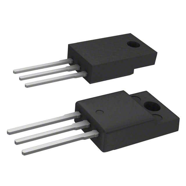
- Package: The STF33N65M2 is typically available in a TO-220 package, which provides thermal efficiency and mechanical robustness.
- Essence: Its essence lies in providing efficient power switching and management capabilities in electronic systems.
- Packaging/Quantity: The STF33N65M2 is commonly packaged in reels or tubes, with varying quantities based on manufacturer specifications.
Specifications
- Voltage Rating: 650V
- Current Rating: 33A
- On-State Resistance: 0.09Ω
- Gate-Source Voltage (Max): ±20V
- Operating Temperature Range: -55°C to 150°C
- Package Type: TO-220
Detailed Pin Configuration
The STF33N65M2 typically features three pins: 1. Gate (G): Input pin for controlling the MOSFET's conductivity. 2. Drain (D): Output pin through which the main current flows. 3. Source (S): Common reference point for the input and output circuits.
Functional Features
- Low On-State Resistance: Enables minimal power dissipation during conduction.
- High Switching Speed: Facilitates rapid switching transitions, suitable for high-frequency applications.
- Low Gate Charge: Allows for efficient control of the MOSFET, reducing drive circuitry complexity.
Advantages and Disadvantages
Advantages
- High efficiency in power conversion applications.
- Suitable for high-frequency switching.
- Low power dissipation due to low on-state resistance.
Disadvantages
- Sensitivity to voltage spikes and transients.
- Requires careful consideration of gate driving circuitry to optimize performance.
Working Principles
The STF33N65M2 operates based on the principles of field-effect transistors, where the application of a voltage at the gate terminal controls the flow of current between the drain and source terminals. By modulating the gate-source voltage, the MOSFET can be switched between its on and off states, enabling efficient power management and switching.
Detailed Application Field Plans
The STF33N65M2 finds extensive use in the following application fields: - Switched-Mode Power Supplies: Utilized for high-efficiency power conversion in SMPS designs. - Motor Control: Enables efficient motor driving in industrial and automotive applications. - Inverters and Converters: Used for DC-AC and DC-DC conversion in renewable energy systems and power electronics.
Detailed and Complete Alternative Models
- STF30N65M5: A comparable MOSFET offering similar performance characteristics.
- IRF3205: An alternative MOSFET with equivalent voltage and current ratings.
- IXFK44N50P: Another option with comparable specifications for power management applications.
In conclusion, the STF33N65M2 power MOSFET serves as a crucial component in modern electronic systems, providing efficient power management and switching capabilities across various applications.
Word Count: 511
技術ソリューションにおける STF33N65M2 の適用に関連する 10 件の一般的な質問と回答をリストします。
What is the maximum drain-source voltage rating of STF33N65M2?
- The maximum drain-source voltage rating of STF33N65M2 is 650V.
What is the continuous drain current rating of STF33N65M2?
- The continuous drain current rating of STF33N65M2 is 33A.
What is the on-resistance (RDS(on)) of STF33N65M2?
- The on-resistance (RDS(on)) of STF33N65M2 is typically 0.065 ohms.
What is the gate threshold voltage of STF33N65M2?
- The gate threshold voltage of STF33N65M2 is typically 2.5V.
What are the typical applications for STF33N65M2?
- STF33N65M2 is commonly used in power supplies, motor control, and high voltage switching applications.
Is STF33N65M2 suitable for use in automotive applications?
- Yes, STF33N65M2 is designed to meet the requirements for automotive applications.
Does STF33N65M2 have built-in protection features?
- STF33N65M2 includes built-in protection against overcurrent and overtemperature conditions.
What is the operating temperature range of STF33N65M2?
- The operating temperature range of STF33N65M2 is -55°C to 150°C.
Can STF33N65M2 be used in high-frequency switching applications?
- Yes, STF33N65M2 is suitable for high-frequency switching due to its low RDS(on) and fast switching characteristics.
Are there any recommended thermal management considerations for using STF33N65M2?
- It is recommended to use proper heatsinking and thermal management techniques to ensure optimal performance and reliability when using STF33N65M2 in high-power applications.