

AAT4280AIJS-3-T1
Product Overview
Category
AAT4280AIJS-3-T1 belongs to the category of integrated circuits (ICs).
Use
This product is commonly used in electronic devices for voltage level shifting and signal conditioning.
Characteristics
- Voltage level shifting capability
- Signal conditioning functionality
- Compact package size
- Low power consumption
- Wide operating temperature range
Package
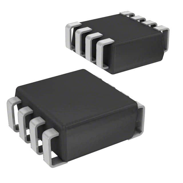
AAT4280AIJS-3-T1 is available in a small outline, surface-mount package (SOT-23-5).
Essence
The essence of AAT4280AIJS-3-T1 lies in its ability to shift voltage levels and condition signals, making it suitable for various applications in the electronics industry.
Packaging/Quantity
This product is typically packaged in reels or tape and reel format, with a quantity of 3000 units per reel.
Specifications
- Input Voltage Range: 1.8V to 5.5V
- Output Voltage Range: 1.8V to 5.5V
- Operating Temperature Range: -40°C to +85°C
- Supply Current: 50µA (typical)
- Rise/Fall Time: 10ns (typical)
- Maximum Output Current: 100mA
Detailed Pin Configuration
AAT4280AIJS-3-T1 has a total of five pins:
- VCC: Power supply input pin.
- VIN: Input voltage pin.
- VOUT: Output voltage pin.
- GND: Ground pin.
- EN: Enable pin for controlling the device's operation.
Functional Features
- Voltage level shifting: The AAT4280AIJS-3-T1 can shift input voltage levels to match the desired output voltage levels.
- Signal conditioning: It provides signal conditioning capabilities, ensuring proper signal integrity and compatibility.
- Low power consumption: The device operates with low power consumption, making it suitable for battery-powered applications.
- Fast response time: It offers a quick rise/fall time, enabling efficient signal processing.
Advantages and Disadvantages
Advantages
- Versatile voltage level shifting capabilities.
- Compact package size allows for easy integration into various electronic devices.
- Wide operating temperature range ensures reliable performance in different environments.
- Low power consumption extends battery life in portable applications.
Disadvantages
- Limited maximum output current may restrict its use in high-power applications.
- Requires careful consideration of input and output voltage ranges to avoid damage or improper operation.
Working Principles
The AAT4280AIJS-3-T1 operates based on the principles of voltage level shifting and signal conditioning. It utilizes internal circuitry to convert input voltages to desired output levels while maintaining signal integrity. The device is controlled by the enable pin (EN), allowing users to activate or deactivate its functionality as needed.
Detailed Application Field Plans
AAT4280AIJS-3-T1 finds applications in various fields, including but not limited to:
- Consumer electronics: Used in smartphones, tablets, and other portable devices for voltage level shifting and signal conditioning.
- Industrial automation: Employed in control systems and sensors for interfacing different voltage levels.
- Automotive electronics: Integrated into automotive modules and systems for signal conditioning and voltage adaptation.
- Internet of Things (IoT): Utilized in IoT devices to ensure compatibility between different voltage domains.
Detailed and Complete Alternative Models
- AAT4280BIJS-3-T1: Similar to AAT4280AIJS-3-T1 but with enhanced features.
- AAT4280CIJS-3-T1: Lower-cost alternative with basic voltage level shifting capabilities.
- AAT4280DIJS-3-T1: High-performance version with extended temperature range.
These alternative models offer similar functionality and can be considered based on specific application requirements.
Word count: 529 words
技術ソリューションにおける AAT4280AIJS-3-T1 の適用に関連する 10 件の一般的な質問と回答をリストします。
Sure! Here are 10 common questions and answers related to the application of AAT4280AIJS-3-T1 in technical solutions:
Q1: What is the AAT4280AIJS-3-T1? A1: The AAT4280AIJS-3-T1 is a specific model of integrated circuit (IC) designed for power management applications.
Q2: What are the typical applications of AAT4280AIJS-3-T1? A2: The AAT4280AIJS-3-T1 is commonly used in various technical solutions such as battery-powered devices, portable electronics, and low-power systems.
Q3: What is the input voltage range supported by AAT4280AIJS-3-T1? A3: The AAT4280AIJS-3-T1 supports an input voltage range from 2.7V to 5.5V.
Q4: What is the output voltage range provided by AAT4280AIJS-3-T1? A4: The AAT4280AIJS-3-T1 can provide an output voltage range from 0.6V to 5.5V.
Q5: What is the maximum output current capability of AAT4280AIJS-3-T1? A5: The AAT4280AIJS-3-T1 has a maximum output current capability of 300mA.
Q6: Does AAT4280AIJS-3-T1 have built-in protection features? A6: Yes, the AAT4280AIJS-3-T1 includes various protection features like overcurrent protection, thermal shutdown, and reverse current protection.
Q7: Can AAT4280AIJS-3-T1 operate in a wide temperature range? A7: Yes, the AAT4280AIJS-3-T1 is designed to operate in a wide temperature range from -40°C to +85°C.
Q8: Is AAT4280AIJS-3-T1 compatible with both NPN and PNP transistors? A8: Yes, the AAT4280AIJS-3-T1 is compatible with both NPN and PNP transistors, providing flexibility in circuit design.
Q9: Does AAT4280AIJS-3-T1 require external components for operation? A9: Yes, the AAT4280AIJS-3-T1 requires a few external components like capacitors and resistors for proper operation.
Q10: What package type does AAT4280AIJS-3-T1 come in? A10: The AAT4280AIJS-3-T1 is available in a small SOT-23 package, which is commonly used for compact electronic designs.
Please note that these questions and answers are based on general information about the AAT4280AIJS-3-T1. For specific technical details and application requirements, it is recommended to refer to the datasheet or consult the manufacturer's documentation.