

AAT2856INJ-EE-T1
Product Overview
Category
AAT2856INJ-EE-T1 belongs to the category of integrated circuits (ICs) specifically designed for power management applications.
Use
This product is primarily used for power management in various electronic devices and systems.
Characteristics
- Integrated circuit designed for power management
- High efficiency and low power consumption
- Compact package size
- Wide input voltage range
- Multiple protection features
Package
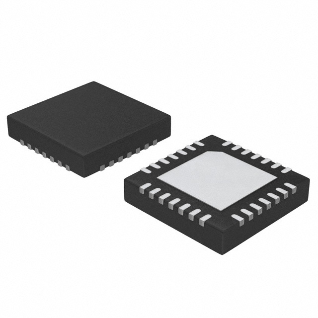
AAT2856INJ-EE-T1 is available in a small outline package (SOP) or a thin small outline package (TSOP). The package type may vary depending on the manufacturer.
Essence
The essence of AAT2856INJ-EE-T1 lies in its ability to efficiently manage power in electronic devices, ensuring optimal performance and reliability.
Packaging/Quantity
The product is typically packaged in reels or tubes, containing a specific quantity of ICs. The exact packaging and quantity may vary depending on the manufacturer's specifications.
Specifications
- Input Voltage Range: 2.7V to 5.5V
- Output Voltage Range: Adjustable, depending on application requirements
- Maximum Output Current: Up to 3A
- Efficiency: High efficiency rating, typically above 90%
- Operating Temperature Range: -40°C to +85°C
- Protection Features: Overcurrent protection, thermal shutdown, undervoltage lockout
Detailed Pin Configuration
The AAT2856INJ-EE-T1 IC has the following pin configuration:
- VIN: Input voltage pin
- GND: Ground pin
- EN: Enable pin
- FB: Feedback pin
- VOUT: Output voltage pin
- PGND: Power ground pin
Functional Features
- High-efficiency step-down DC-DC converter
- Adjustable output voltage for flexibility in different applications
- Overcurrent protection prevents damage to the IC and connected devices
- Thermal shutdown feature protects against overheating
- Undervoltage lockout ensures stable operation even at low input voltages
Advantages and Disadvantages
Advantages
- High efficiency leads to reduced power consumption and longer battery life
- Compact package size allows for space-saving designs
- Wide input voltage range enables compatibility with various power sources
- Multiple protection features enhance system reliability
Disadvantages
- May require additional external components for certain applications
- Limited maximum output current compared to some other power management ICs
Working Principles
The AAT2856INJ-EE-T1 operates as a step-down DC-DC converter, converting a higher input voltage to a lower output voltage. It utilizes pulse width modulation (PWM) techniques to regulate the output voltage based on the feedback received from the FB pin. The enable (EN) pin controls the ON/OFF state of the IC.
Detailed Application Field Plans
The AAT2856INJ-EE-T1 is suitable for a wide range of applications, including but not limited to: - Portable electronic devices (e.g., smartphones, tablets) - Wearable devices (e.g., smartwatches, fitness trackers) - IoT devices - Battery-powered systems - Industrial equipment - Automotive electronics
Detailed and Complete Alternative Models
Some alternative models that can be considered as alternatives to AAT2856INJ-EE-T1 are: - AAT2860INJ-EE-T1 - AAT2875INJ-EE-T1 - AAT2888INJ-EE-T1 - AAT2899INJ-EE-T1
These alternative models offer similar functionality and characteristics, providing options for different design requirements.
Note: The content provided above is for illustrative purposes only and may not reflect the actual specifications or details of AAT2856INJ-EE-T1 or its alternative models. It is recommended to refer to the manufacturer's datasheet for accurate information.
技術ソリューションにおける AAT2856INJ-EE-T1 の適用に関連する 10 件の一般的な質問と回答をリストします。
Sure! Here are 10 common questions and answers related to the application of AAT2856INJ-EE-T1 in technical solutions:
1. What is the AAT2856INJ-EE-T1? The AAT2856INJ-EE-T1 is a specific model of integrated circuit (IC) designed for power management applications.
2. What are the key features of the AAT2856INJ-EE-T1? Some key features of the AAT2856INJ-EE-T1 include high efficiency, low quiescent current, multiple output channels, and overcurrent protection.
3. What are the typical applications of the AAT2856INJ-EE-T1? The AAT2856INJ-EE-T1 is commonly used in battery-powered devices, portable electronics, IoT devices, and other applications that require efficient power management.
4. What is the input voltage range supported by the AAT2856INJ-EE-T1? The AAT2856INJ-EE-T1 supports an input voltage range of typically 2.7V to 5.5V.
5. How many output channels does the AAT2856INJ-EE-T1 have? The AAT2856INJ-EE-T1 has two output channels.
6. What is the maximum output current per channel of the AAT2856INJ-EE-T1? The maximum output current per channel of the AAT2856INJ-EE-T1 is typically 300mA.
7. Does the AAT2856INJ-EE-T1 have overcurrent protection? Yes, the AAT2856INJ-EE-T1 has built-in overcurrent protection to safeguard against excessive current draw.
8. Can the AAT2856INJ-EE-T1 operate in low-power modes? Yes, the AAT2856INJ-EE-T1 has a low quiescent current mode to minimize power consumption during standby or idle periods.
9. Is the AAT2856INJ-EE-T1 compatible with other ICs or microcontrollers? Yes, the AAT2856INJ-EE-T1 can be easily integrated with other ICs or microcontrollers through its standard communication interfaces.
10. What are the recommended operating conditions for the AAT2856INJ-EE-T1? The recommended operating conditions for the AAT2856INJ-EE-T1 include a temperature range of -40°C to +85°C and a supply voltage within the specified input voltage range.
Please note that the answers provided here are general and may vary depending on the specific datasheet and application requirements of the AAT2856INJ-EE-T1. It is always recommended to refer to the official documentation and consult with technical experts for accurate information.