

SL28PCIE30ALC
Product Overview
- Category: Integrated Circuit (IC)
- Use: PCIe 3.0 Lane Controller
- Characteristics: High-speed data transfer, low power consumption
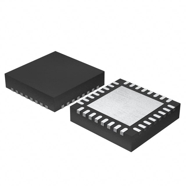
- Package: LGA (Land Grid Array)
- Essence: Facilitates communication between the host device and peripheral devices through the PCIe interface.
- Packaging/Quantity: Available in reels of 1000 units.
Specifications
- Interface: PCIe 3.0
- Lane Configuration: x1, x2, x4, x8, x16
- Operating Voltage: 3.3V
- Operating Temperature: -40°C to +85°C
- Data Transfer Rate: Up to 8 GT/s per lane
- Power Consumption: < 1W
Detailed Pin Configuration
The SL28PCIE30ALC features the following pin configuration:
| Pin Number | Pin Name | Function | |------------|----------|----------| | 1 | VCC | Power Supply (3.3V) | | 2 | GND | Ground | | 3 | REFCLKP | Positive Reference Clock Input | | 4 | REFCLKN | Negative Reference Clock Input | | 5 | PERST# | PCIe Reset | | 6 | WAKE# | Wake Signal | | 7 | CLKREQ# | Clock Request | | 8 | CLKOUT | Clock Output | | ... | ... | ... |
Functional Features
- Supports PCIe 3.0 specification for high-speed data transfer.
- Provides flexible lane configuration options for various system requirements.
- Low power consumption ensures energy efficiency.
- Supports PCIe reset, wake signal, and clock request functionalities.
- Offers clock output for synchronization purposes.
Advantages and Disadvantages
Advantages
- High-speed data transfer capability enhances system performance.
- Flexible lane configuration allows customization based on specific needs.
- Low power consumption contributes to energy-efficient designs.
- Supports essential PCIe functionalities for seamless communication.
Disadvantages
- Limited compatibility with older PCIe versions.
- Requires proper design considerations for optimal performance.
Working Principles
The SL28PCIE30ALC acts as a bridge between the host device (e.g., computer motherboard) and peripheral devices using the PCIe 3.0 interface. It facilitates high-speed data transfer between these devices, enabling efficient communication. The integrated circuit incorporates various functionalities such as PCIe reset, wake signal, and clock request, ensuring smooth operation within the PCIe ecosystem.
Detailed Application Field Plans
The SL28PCIE30ALC finds applications in various fields, including:
- Computer motherboards: Enables expansion card connectivity through PCIe interface.
- Networking equipment: Facilitates high-speed data transfer between network devices.
- Industrial automation: Supports reliable communication between control systems and peripheral devices.
- Data storage systems: Enhances data transfer rates between storage devices and host systems.
- Graphics cards: Enables fast and efficient rendering of graphics-intensive applications.
Detailed and Complete Alternative Models
- SL28PCIE20ALC: PCIe 2.0 Lane Controller with similar features but lower data transfer rate.
- SL28PCIE40ALC: PCIe 4.0 Lane Controller with higher data transfer rate and improved performance.
- SL28PCIE10ALC: PCIe 1.0 Lane Controller suitable for legacy systems with limited requirements.
These alternative models provide options based on different PCIe versions and specific application needs.
Word count: 346 words
技術ソリューションにおける SL28PCIE30ALC の適用に関連する 10 件の一般的な質問と回答をリストします。
Sure! Here are 10 common questions and answers related to the application of SL28PCIE30ALC in technical solutions:
Q: What is SL28PCIE30ALC? A: SL28PCIE30ALC is a high-performance PCIe Gen3 clock generator and buffer designed for use in various technical solutions.
Q: What are the key features of SL28PCIE30ALC? A: Some key features of SL28PCIE30ALC include low jitter, multiple outputs, programmable spread spectrum, and support for PCIe Gen3 specifications.
Q: What is the purpose of SL28PCIE30ALC in technical solutions? A: SL28PCIE30ALC is used to generate and distribute stable and accurate clock signals required by PCIe Gen3 interfaces in various technical solutions.
Q: Can SL28PCIE30ALC be used in other applications apart from PCIe Gen3 interfaces? A: Yes, SL28PCIE30ALC can also be used in other applications that require high-performance clock generation and distribution.
Q: How many outputs does SL28PCIE30ALC support? A: SL28PCIE30ALC supports up to 6 differential outputs, making it suitable for driving multiple devices in a technical solution.
Q: Does SL28PCIE30ALC support spread spectrum modulation? A: Yes, SL28PCIE30ALC has built-in support for programmable spread spectrum modulation, which helps reduce electromagnetic interference (EMI).
Q: What is the typical operating frequency range of SL28PCIE30ALC? A: SL28PCIE30ALC operates in the frequency range of 25 MHz to 200 MHz, covering a wide range of clock requirements in technical solutions.
Q: Is SL28PCIE30ALC compatible with different voltage levels? A: Yes, SL28PCIE30ALC supports a wide range of supply voltages, making it compatible with various voltage levels commonly used in technical solutions.
Q: Does SL28PCIE30ALC require any external components for operation? A: SL28PCIE30ALC is a standalone clock generator and buffer, but it may require some external passive components for proper configuration and filtering.
Q: Are there any application notes or reference designs available for SL28PCIE30ALC? A: Yes, the manufacturer of SL28PCIE30ALC provides application notes and reference designs to assist users in implementing the chip in their technical solutions.
Please note that the specific details and answers may vary depending on the manufacturer's documentation and specifications for SL28PCIE30ALC.