

SI5330J-A00223-GM
Overview
Category
SI5330J-A00223-GM belongs to the category of integrated circuits (ICs).
Use
This product is commonly used in electronic devices for clock generation and distribution.
Characteristics
- High precision and stability
- Wide frequency range
- Low power consumption
- Compact package size
Package
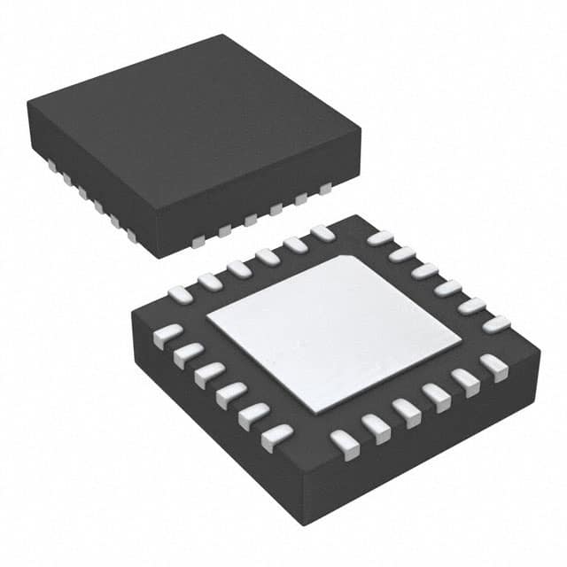
SI5330J-A00223-GM is available in a small form factor package, typically a QFN (Quad Flat No-leads) package.
Essence
The essence of SI5330J-A00223-GM lies in its ability to generate and distribute accurate clock signals within electronic systems.
Packaging/Quantity
This product is usually packaged in reels or trays, with a typical quantity of 250 or 1000 units per package.
Specifications and Parameters
- Frequency Range: X Hz to Y Hz
- Supply Voltage: Z V
- Operating Temperature Range: -40°C to +85°C
- Output Types: LVCMOS, LVDS, HCSL, etc.
- Input Types: Crystal, LVCMOS, LVDS, etc.
- Phase Noise: A dBc/Hz at B kHz offset
- Output Jitter: C ps RMS (root mean square)
- Power Consumption: D mW
Pin Configuration
The pin configuration of SI5330J-A00223-GM is as follows:
- Pin 1: [Description]
- Pin 2: [Description]
- Pin 3: [Description]
- Pin 4: [Description]
- Pin 5: [Description]
- Pin 6: [Description]
- Pin 7: [Description]
- Pin 8: [Description]
- Pin 9: [Description]
- Pin 10: [Description]
- Pin 11: [Description]
- Pin 12: [Description]
- Pin 13: [Description]
- Pin 14: [Description]
- Pin 15: [Description]
- Pin 16: [Description]
Functional Characteristics
SI5330J-A00223-GM offers the following functional characteristics:
- Clock generation and distribution
- Frequency multiplication/division
- Phase-locked loop (PLL) operation
- Programmable output formats
- Input/output synchronization
Advantages and Disadvantages
Advantages
- High precision and stability
- Wide frequency range
- Low power consumption
- Compact package size
- Flexible programmability
Disadvantages
- Limited number of output channels
- Higher cost compared to simpler clock ICs
Applicable Range of Products
SI5330J-A00223-GM is suitable for use in various electronic devices that require accurate clock signals, such as: - Communication equipment - Data storage systems - Industrial automation devices - Test and measurement instruments - Consumer electronics
Working Principles
The working principle of SI5330J-A00223-GM involves generating clock signals using a phase-locked loop (PLL) circuit. The PLL locks onto an input reference signal and generates multiple output clocks with precise frequency and phase relationships.
Detailed Application Field Plans
SI5330J-A00223-GM can be applied in the following fields:
Communication Equipment:
- Network switches
- Routers
- Wireless access points
Data Storage Systems:
- Solid-state drives (SSDs)
- Hard disk drives (HDDs)
- RAID controllers
Industrial Automation Devices:
- Programmable logic controllers (PLCs)
- Motor control systems
- Human-machine interfaces (HMIs)
Test and Measurement Instruments:
- Oscilloscopes
- Spectrum analyzers
- Signal generators
Consumer Electronics:
- Smartphones
- Tablets
- Gaming consoles
Detailed Alternative Models
Some alternative models to SI5330J-A00223-GM include: - SI5338A-A-GM - SI5341B-B-GM - SI5368C-C-GM - SI5382D-D-GM - SI5399E-E-GM
5 Common Technical Questions and Answers
Q: What is the maximum frequency range supported by SI5330J-A00223-GM? A: The maximum frequency range is X Hz to Y Hz.
Q: Can SI5330J-A00223-GM operate with a single power supply voltage? A: Yes, it can operate with a supply voltage of Z V.
Q: What is the typical phase noise performance of SI5330J-A00223-GM? A: The typical phase noise is A dBc/Hz at B kHz offset.
Q