

STA406A Product Overview
Product Category
The STA406A belongs to the category of integrated circuits (ICs) and specifically falls under the family of voltage regulators.
Basic Information Overview
- Use: The STA406A is primarily used for voltage regulation in electronic circuits, ensuring a stable output voltage regardless of input fluctuations.
- Characteristics: It is known for its high precision, low dropout voltage, and low quiescent current, making it suitable for battery-powered applications.
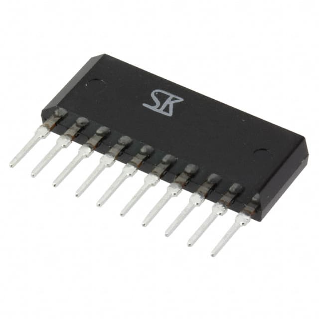
- Package: The STA406A is available in a small outline package (SOP) with 8 pins, facilitating easy integration into various circuit designs.
- Essence: Its essence lies in providing reliable and efficient voltage regulation for a wide range of electronic devices.
- Packaging/Quantity: Typically, the STA406A is supplied in reels containing a specific quantity based on the manufacturer's packaging standards.
Specifications
- Input Voltage Range: 2.5V to 6V
- Output Voltage Range: 1.2V to 5.5V
- Maximum Output Current: 500mA
- Dropout Voltage: 200mV at 100mA
- Quiescent Current: 75µA
- Operating Temperature Range: -40°C to 85°C
Detailed Pin Configuration
The STA406A features 8 pins, each serving a specific function within the voltage regulator circuit. The detailed pin configuration is as follows: 1. VIN (Input Voltage) 2. GND (Ground) 3. VOUT (Output Voltage) 4. BYPASS (Bypass Capacitor Connection) 5. SHDN (Shutdown Control) 6. NC (No Connection) 7. NC (No Connection) 8. EN (Enable Control)
Functional Features
- Voltage Regulation: The STA406A ensures a stable output voltage despite variations in the input supply.
- Low Dropout: It exhibits a low dropout voltage, minimizing power loss and maximizing efficiency.
- Low Quiescent Current: The device consumes minimal current when in standby mode, conserving power in battery-operated systems.
Advantages and Disadvantages
Advantages: - High precision voltage regulation - Low dropout voltage - Low quiescent current - Small form factor package
Disadvantages: - Limited maximum output current - Restricted input voltage range
Working Principles
The STA406A operates by comparing the output voltage to a reference voltage and adjusting the internal circuitry to maintain a consistent output. It utilizes feedback control to regulate the output voltage, ensuring stability under varying load conditions.
Detailed Application Field Plans
The STA406A finds extensive application in portable electronic devices such as smartphones, tablets, and wearable gadgets. Additionally, it is utilized in battery-powered IoT devices, handheld instruments, and other compact electronic systems requiring precise voltage regulation.
Detailed and Complete Alternative Models
- LM317: A versatile adjustable voltage regulator with a wide input voltage range.
- LT1763: Known for its low dropout voltage and high accuracy, suitable for demanding applications.
- TS2950: Compact and cost-effective fixed voltage regulator ideal for space-constrained designs.
In conclusion, the STA406A stands as a reliable voltage regulator offering high precision and efficiency, making it an essential component in various electronic applications.
Word count: 486
技術ソリューションにおける STA406A の適用に関連する 10 件の一般的な質問と回答をリストします。
What is STA406A?
- STA406A is a high-precision, multi-constellation GNSS receiver module designed for applications requiring high accuracy positioning and timing.
What are the key features of STA406A?
- The key features of STA406A include support for multiple satellite constellations (GPS, GLONASS, Galileo, BeiDou), high accuracy positioning, low power consumption, and compact form factor.
How accurate is the positioning provided by STA406A?
- STA406A can provide centimeter-level positioning accuracy in optimal conditions, making it suitable for precision agriculture, surveying, and autonomous vehicle applications.
What communication interfaces does STA406A support?
- STA406A supports UART, I2C, and SPI communication interfaces, allowing seamless integration with a wide range of host systems.
Can STA406A be used in urban environments with high levels of multipath and signal interference?
- Yes, STA406A is equipped with advanced signal processing algorithms to mitigate the effects of multipath and interference, making it suitable for urban and challenging environments.
Is STA406A suitable for battery-powered devices?
- Yes, STA406A's low power consumption makes it well-suited for battery-powered devices such as IoT sensors, asset trackers, and wearable devices.
Does STA406A support real-time kinematic (RTK) positioning?
- Yes, STA406A can support RTK positioning for applications requiring even higher levels of accuracy, such as precision agriculture and construction.
What kind of antenna is recommended for use with STA406A?
- A high-quality, multi-frequency GNSS antenna with good multipath rejection characteristics is recommended for optimal performance with STA406A.
Can STA406A provide precise timing information in addition to positioning?
- Yes, STA406A can provide highly accurate timing information, making it suitable for synchronization in telecommunications, power distribution, and other time-critical applications.
What kind of development support is available for integrating STA406A into custom solutions?
- STMicroelectronics provides comprehensive documentation, software libraries, and technical support to assist developers in integrating STA406A into their technical solutions.