

商品詳細は仕様をご覧ください。
UPA2813T1L-E1-AT
Introduction
The UPA2813T1L-E1-AT is a crucial component in the field of electronic devices, offering a wide range of applications and functionalities. This entry provides an in-depth overview of the UPA2813T1L-E1-AT, including its product category, basic information, specifications, pin configuration, functional features, advantages and disadvantages, working principles, application field plans, and alternative models.
Product Category
The UPA2813T1L-E1-AT belongs to the category of integrated circuits (ICs), specifically within the power management ICs segment.
Basic Information Overview
- Use: The UPA2813T1L-E1-AT is primarily used for power management and voltage regulation in various electronic devices.
- Characteristics: It is known for its high efficiency, low power consumption, and compact design.
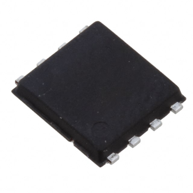
- Package: The UPA2813T1L-E1-AT is typically available in a small outline package (SOP) or thin small outline package (TSOP).
- Essence: Its essence lies in providing stable and regulated power supply to electronic systems.
- Packaging/Quantity: It is commonly packaged in reels with varying quantities based on customer requirements.
Specifications
The UPA2813T1L-E1-AT features the following specifications: - Input Voltage Range: 4.5V to 28V - Output Voltage Range: 0.8V to 24V - Maximum Output Current: 3A - Operating Temperature Range: -40°C to 125°C - Control Interface: PWM
Detailed Pin Configuration
The UPA2813T1L-E1-AT has a detailed pin configuration as follows: 1. VIN (Input Voltage) 2. GND (Ground) 3. EN (Enable) 4. FB (Feedback) 5. COMP (Compensation) 6. SS (Soft Start) 7. PGND (Power Ground) 8. VOUT (Output Voltage)
Functional Features
The key functional features of the UPA2813T1L-E1-AT include: - Wide input voltage range for versatile applications - High efficiency and low dropout voltage - Overcurrent and thermal protection - Adjustable output voltage through external resistors - Soft start function for controlled power-up sequencing
Advantages and Disadvantages
Advantages
- High efficiency leads to reduced power dissipation
- Wide input voltage range enhances flexibility in system design
- Comprehensive protection features ensure device reliability
Disadvantages
- Limited maximum output current compared to some competing models
- Sensitive to external noise due to high-frequency operation
Working Principles
The UPA2813T1L-E1-AT operates based on pulse-width modulation (PWM) control to regulate the output voltage. When enabled, it compares the feedback voltage with a reference voltage to adjust the duty cycle of the internal switch, thereby maintaining the desired output voltage.
Detailed Application Field Plans
The UPA2813T1L-E1-AT finds extensive application in various fields, including: - Consumer electronics: Power supplies for smartphones, tablets, and portable devices - Industrial automation: Motor control, LED lighting, and distributed power systems - Automotive: Onboard chargers, infotainment systems, and advanced driver-assistance systems
Detailed and Complete Alternative Models
For users seeking alternatives to the UPA2813T1L-E1-AT, several comparable models are available from different manufacturers, such as: - Texas Instruments TPS54332 - Analog Devices ADP2384 - ON Semiconductor NCP1562
In conclusion, the UPA2813T1L-E1-AT stands as a vital component in the realm of power management ICs, offering a balance of efficiency, versatility, and protection features. Its widespread applicability and availability of alternative models make it a significant consideration for diverse electronic designs.
[Word Count: 598]
技術ソリューションにおける UPA2813T1L-E1-AT の適用に関連する 10 件の一般的な質問と回答をリストします。
What is the UPA2813T1L-E1-AT used for?
- The UPA2813T1L-E1-AT is a high-speed, low-side gate driver IC designed for use in applications such as motor control, power supplies, and inverters.
What is the maximum operating voltage of the UPA2813T1L-E1-AT?
- The UPA2813T1L-E1-AT has a maximum operating voltage of 600V.
What is the maximum peak output current of the UPA2813T1L-E1-AT?
- The UPA2813T1L-E1-AT has a maximum peak output current of 4A.
What type of load can the UPA2813T1L-E1-AT drive?
- The UPA2813T1L-E1-AT can drive capacitive, inductive, and resistive loads.
Does the UPA2813T1L-E1-AT have built-in protection features?
- Yes, the UPA2813T1L-E1-AT includes built-in undervoltage lockout (UVLO) and overcurrent protection.
What is the input logic voltage level for the UPA2813T1L-E1-AT?
- The UPA2813T1L-E1-AT operates with input logic voltage levels compatible with standard CMOS or TTL logic signals.
Can the UPA2813T1L-E1-AT be used in automotive applications?
- Yes, the UPA2813T1L-E1-AT is suitable for automotive applications, including motor control and power management.
What is the recommended operating temperature range for the UPA2813T1L-E1-AT?
- The UPA2813T1L-E1-AT is designed to operate within a temperature range of -40°C to 125°C.
Is the UPA2813T1L-E1-AT RoHS compliant?
- Yes, the UPA2813T1L-E1-AT is compliant with the Restriction of Hazardous Substances (RoHS) directive.
Are there any application notes or reference designs available for the UPA2813T1L-E1-AT?
- Yes, application notes and reference designs are available from the manufacturer to assist with the implementation of the UPA2813T1L-E1-AT in various technical solutions.