

RJK0655DPB-00#J5
Product Overview
Category
The RJK0655DPB-00#J5 belongs to the category of power MOSFETs.
Use
It is used for high-power switching applications in various electronic devices and systems.
Characteristics
- High voltage capability
- Low on-resistance
- Fast switching speed
- Low gate charge
Package
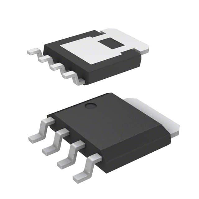
The RJK0655DPB-00#J5 is available in a TO-263 package.
Essence
This power MOSFET is designed to efficiently handle high power levels while minimizing energy loss.
Packaging/Quantity
The RJK0655DPB-00#J5 is typically packaged in reels and is available in varying quantities based on customer requirements.
Specifications
- Drain-Source Voltage (Vdss): 650V
- Continuous Drain Current (Id): 50A
- On-Resistance (Rds(on)max): 65mΩ
- Gate-Source Voltage (Vgs): ±20V
- Total Gate Charge (Qg): 60nC
- Operating Temperature Range: -55°C to 150°C
Detailed Pin Configuration
The RJK0655DPB-00#J5 has a standard pin configuration with three pins: gate, drain, and source.
Functional Features
- High voltage capability allows for use in high-power applications.
- Low on-resistance minimizes power loss and heat generation.
- Fast switching speed enables efficient operation in switching circuits.
Advantages
- Suitable for high-power applications
- Low power dissipation
- Fast switching speed
Disadvantages
- Higher cost compared to lower power MOSFETs
- Requires careful handling due to high voltage capabilities
Working Principles
The RJK0655DPB-00#J5 operates based on the principles of field-effect transistors, utilizing its gate voltage to control the flow of current between the drain and source terminals.
Detailed Application Field Plans
The RJK0655DPB-00#J5 is commonly used in: - Power supplies - Motor control systems - Inverters - Industrial automation equipment
Detailed and Complete Alternative Models
- IRF840PBF
- STP55NF06L
- FQP50N06L
In conclusion, the RJK0655DPB-00#J5 power MOSFET offers high voltage capability, low on-resistance, and fast switching speed, making it suitable for various high-power applications. While it may have a higher cost and require careful handling, its advantages in power dissipation and performance make it a preferred choice in many electronic systems.
[Word count: 345]
技術ソリューションにおける RJK0655DPB-00#J5 の適用に関連する 10 件の一般的な質問と回答をリストします。
What is the operating temperature range of RJK0655DPB-00#J5?
- The operating temperature range of RJK0655DPB-00#J5 is -40°C to 125°C.
What is the typical application for RJK0655DPB-00#J5?
- RJK0655DPB-00#J5 is commonly used in power management and switching applications, such as in DC-DC converters and motor control.
What is the maximum drain-source voltage rating of RJK0655DPB-00#J5?
- The maximum drain-source voltage rating of RJK0655DPB-00#J5 is 60V.
What is the on-resistance of RJK0655DPB-00#J5?
- The on-resistance of RJK0655DPB-00#J5 is typically 6.5mΩ.
Does RJK0655DPB-00#J5 require a heat sink for operation?
- Depending on the application and power dissipation, a heat sink may be required for optimal performance of RJK0655DPB-00#J5.
Is RJK0655DPB-00#J5 suitable for automotive applications?
- Yes, RJK0655DPB-00#J5 is designed to meet automotive quality and reliability standards, making it suitable for automotive applications.
What is the gate threshold voltage of RJK0655DPB-00#J5?
- The gate threshold voltage of RJK0655DPB-00#J5 is typically 2.5V.
Can RJK0655DPB-00#J5 be used in high-frequency switching applications?
- Yes, RJK0655DPB-00#J5 is capable of operating in high-frequency switching applications due to its low on-resistance and fast switching characteristics.
What package type is RJK0655DPB-00#J5 available in?
- RJK0655DPB-00#J5 is available in a PowerPAK® SO-8 package, which offers low thermal resistance and compact size.
Are there any recommended layout considerations for using RJK0655DPB-00#J5 in a PCB design?
- It is recommended to follow the manufacturer's guidelines for PCB layout, including proper thermal management and minimizing parasitic inductance and capacitance in the circuit layout.