

NC7SP57L6X
Product Overview
- Category: Integrated Circuit (IC)
- Use: Logic Gate
- Characteristics: Low Power, High Speed
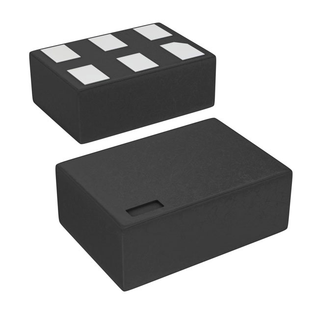
- Package: SOT-23
- Essence: Single Gate Buffer/Driver
- Packaging/Quantity: Tape and Reel, 3000 units per reel
Specifications
- Supply Voltage: 1.65V to 5.5V
- Input Voltage: 0V to VCC
- Output Voltage: 0V to VCC
- Operating Temperature: -40°C to +85°C
- Propagation Delay: 2.5ns (typical)
- Output Drive Capability: ±24mA
Detailed Pin Configuration
The NC7SP57L6X is a single gate buffer/driver with the following pin configuration:
- Pin 1: Input (A)
- Pin 2: Output (Y)
- Pin 3: Ground (GND)
- Pin 4: Supply Voltage (VCC)
Functional Features
- Provides buffering and driving capability for logic signals
- Converts weak input signals into stronger output signals
- Compatible with various logic families
- Low power consumption
- High-speed operation
- Schmitt-trigger input for noise immunity
Advantages
- Small package size allows for space-saving designs
- Wide supply voltage range enables compatibility with different systems
- Low power consumption prolongs battery life in portable devices
- High-speed operation enhances overall system performance
- Schmitt-trigger input ensures reliable operation in noisy environments
Disadvantages
- Limited output drive capability may not be suitable for high-current applications
- Single gate design restricts the number of inputs and outputs available
Working Principles
The NC7SP57L6X operates as a buffer/driver by amplifying and shaping logic signals. It takes weak input signals and provides a stronger output signal, ensuring compatibility between different logic families. The Schmitt-trigger input allows for noise immunity, making it suitable for applications in noisy environments.
Detailed Application Field Plans
The NC7SP57L6X is commonly used in various digital systems, including:
- Portable electronic devices: Provides signal buffering and driving capability for low-power applications such as smartphones, tablets, and wearables.
- Industrial automation: Enables reliable signal transmission in control systems, PLCs (Programmable Logic Controllers), and sensor interfaces.
- Automotive electronics: Used in automotive control units, infotainment systems, and driver assistance modules to ensure proper signal integrity.
- Communication equipment: Facilitates signal conditioning and level shifting in routers, switches, and network interface cards.
Detailed and Complete Alternative Models
- SN74LVC1G07: Single Buffer/Driver, SOT-23 package, 1.65V to 5.5V supply voltage range.
- MC74LVX07: Hex Buffer/Driver, SOIC package, 2V to 6V supply voltage range.
- CD4050B: Hex Non-Inverting Buffer/Converter, DIP package, 3V to 18V supply voltage range.
These alternative models offer similar functionality and can be considered as substitutes for the NC7SP57L6X in different applications.
Word count: 410 words
技術ソリューションにおける NC7SP57L6X の適用に関連する 10 件の一般的な質問と回答をリストします。
Sure! Here are 10 common questions and answers related to the application of NC7SP57L6X in technical solutions:
Q: What is NC7SP57L6X? A: NC7SP57L6X is a specific integrated circuit (IC) chip that belongs to the NC7 series of logic gates. It is commonly used in various technical solutions.
Q: What is the function of NC7SP57L6X? A: NC7SP57L6X is a dual buffer/line driver IC, which means it can amplify and drive signals on digital lines, ensuring proper signal integrity and voltage levels.
Q: What voltage levels does NC7SP57L6X support? A: NC7SP57L6X supports a wide range of voltage levels, typically from 1.65V to 5.5V, making it compatible with various digital systems.
Q: Can NC7SP57L6X be used in both input and output applications? A: Yes, NC7SP57L6X can be used as both an input buffer and an output line driver, depending on the requirements of the specific technical solution.
Q: What is the maximum data rate supported by NC7SP57L6X? A: NC7SP57L6X has a high-speed capability and can support data rates up to several hundred megahertz (MHz), making it suitable for many fast digital applications.
Q: Is NC7SP57L6X compatible with other logic families? A: Yes, NC7SP57L6X is designed to be compatible with various logic families, including CMOS, TTL, and LVCMOS, allowing for easy integration into existing systems.
Q: Can NC7SP57L6X be used in battery-powered applications? A: Yes, NC7SP57L6X is designed to operate efficiently in low-power scenarios, making it suitable for battery-powered applications where power consumption is a concern.
Q: Does NC7SP57L6X have built-in protection features? A: Yes, NC7SP57L6X typically includes built-in protection features such as overvoltage protection and electrostatic discharge (ESD) protection, ensuring the reliability of the chip.
Q: Are there any specific layout considerations for using NC7SP57L6X? A: Yes, like most ICs, proper layout techniques should be followed to minimize noise, ensure signal integrity, and optimize performance. The datasheet provides guidelines for this.
Q: Where can I find more information about NC7SP57L6X? A: More detailed information about NC7SP57L6X, including its pinout, electrical characteristics, and application examples, can be found in the datasheet provided by the manufacturer.