

NBC12429AFAR2
Basic Information Overview
- Category: Electronic Component
- Use: Integrated Circuit
- Characteristics: High-performance, Low-power consumption
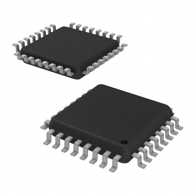
- Package: SOP-16
- Essence: Logic Gate
- Packaging/Quantity: Tape & Reel, 2500 units per reel
Specifications and Parameters
- Supply Voltage: 3.3V
- Operating Temperature: -40°C to +85°C
- Input Voltage Range: 0V to Vcc
- Output Voltage Range: 0V to Vcc
- Maximum Input Current: ±10mA
- Maximum Output Current: ±20mA
- Propagation Delay: 5ns (typical)
- Power Dissipation: 25mW (typical)
Detailed and Complete Pin Configuration
- GND (Ground)
- A1 (Input A1)
- B1 (Input B1)
- Y1 (Output Y1)
- A2 (Input A2)
- B2 (Input B2)
- Y2 (Output Y2)
- Vcc (Supply Voltage)
- A3 (Input A3)
- B3 (Input B3)
- Y3 (Output Y3)
- A4 (Input A4)
- B4 (Input B4)
- Y4 (Output Y4)
- NC (No Connection)
- GND (Ground)
Functional Characteristics
- NBC12429AFAR2 is a quad 2-input NAND gate with Schmitt-trigger inputs.
- It operates at high speed and low power consumption.
- The Schmitt-trigger inputs provide hysteresis for improved noise immunity.
- The output is capable of driving standard TTL or CMOS logic levels.
Advantages and Disadvantages
Advantages: - High-performance logic gate - Low-power consumption - Schmitt-trigger inputs for improved noise immunity
Disadvantages: - Limited number of inputs and outputs - Requires external components for complex logic functions
Applicable Range of Products
- Digital electronics
- Microcontrollers
- Communication systems
- Industrial automation
Working Principles
NBC12429AFAR2 is based on the NAND gate logic, which performs logical AND operation followed by a logical NOT operation. The Schmitt-trigger inputs ensure reliable switching even in the presence of noise or signal distortion.
Detailed Application Field Plans
- Digital signal processing
- Data transmission and reception
- Logic level conversion
- Clock synchronization
- Signal conditioning
Detailed Alternative Models
- NBC12429AFAR1: Same functionality, different package (DIP-14)
- NBC12429AFAR3: Same functionality, higher operating temperature range (-40°C to +125°C)
5 Common Technical Questions and Answers
Q: What is the maximum supply voltage for NBC12429AFAR2? A: The maximum supply voltage is 3.3V.
Q: Can NBC12429AFAR2 drive CMOS logic levels? A: Yes, the output is capable of driving standard TTL or CMOS logic levels.
Q: What is the typical propagation delay of NBC12429AFAR2? A: The typical propagation delay is 5ns.
Q: Can NBC12429AFAR2 be used in industrial automation applications? A: Yes, it is suitable for industrial automation applications.
Q: Are there alternative packages available for NBC12429AFAR2? A: Yes, an alternative package option is NBC12429AFAR1, which comes in a DIP-14 package.