

NB7V586MMNG
Basic Information Overview
- Category: Integrated Circuit
- Use: Signal Conditioning and Clock Generation
- Characteristics: High-speed, Low-power, Differential Input/Output
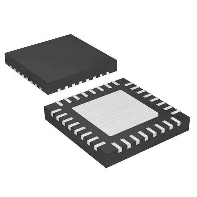
- Package: QFN (Quad Flat No-leads)
- Essence: Signal Integrity Enhancement
- Packaging/Quantity: Tape and Reel, 2500 units per reel
Specifications and Parameters
- Supply Voltage: 2.375V to 3.465V
- Input Voltage Range: -0.5V to VCC+0.5V
- Output Voltage Range: 0V to VCC
- Operating Temperature Range: -40°C to +85°C
- Data Rate: Up to 6.4 Gbps
- Power Consumption: 65 mW (typical)
Detailed and Complete Pin Configuration
- VCC
- GND
- INP
- INN
- OUTN
- OUTP
- SEL
- NC
Functional Characteristics
- Differential Input/Output
- Programmable Output Swing
- Adjustable Input Termination
- Built-in Equalization
- Low Jitter Generation
- CML (Current Mode Logic) Interface
Advantages and Disadvantages
Advantages: - High-speed data transmission - Low power consumption - Excellent signal integrity - Flexible output swing control - Wide operating temperature range
Disadvantages: - Limited input voltage range - Requires external termination resistors - Not suitable for single-ended applications
Applicable Range of Products
- High-speed communication systems
- Data centers
- Networking equipment
- Test and measurement instruments
- Industrial automation
Working Principles
The NB7V586MMNG is a high-speed signal conditioning and clock generation IC. It operates by receiving differential input signals and providing conditioned differential output signals. The IC incorporates built-in equalization and adjustable input termination to enhance signal integrity. It also allows for programmable output swing control, enabling compatibility with various interface standards.
Detailed Application Field Plans
- High-speed data transmission in telecommunications infrastructure.
- Clock generation and distribution in networking equipment.
- Signal conditioning in test and measurement instruments.
- Interface conversion in industrial automation systems.
- Signal integrity enhancement in data centers.
Detailed Alternative Models
- NB7V586MNG: Similar specifications and pin configuration, but without built-in equalization.
- NB7V586MMN: Lower power consumption variant with reduced data rate capability.
- NB7V586MMNR2G: RoHS-compliant version with the same features and performance.
5 Common Technical Questions and Answers
Q: What is the maximum data rate supported by NB7V586MMNG? A: The IC supports data rates up to 6.4 Gbps.
Q: Can I use NB7V586MMNG in single-ended applications? A: No, the IC is designed for differential signaling and is not suitable for single-ended applications.
Q: How do I adjust the output swing of NB7V586MMNG? A: The output swing can be programmed using the SEL pin.
Q: What is the operating temperature range of NB7V586MMNG? A: The IC can operate in temperatures ranging from -40°C to +85°C.
Q: Are external termination resistors required for NB7V586MMNG? A: Yes, external termination resistors are necessary for proper operation of the IC.