

NB4L6254FAR2G
Basic Information Overview
- Category: Integrated Circuit (IC)
- Use: Signal Conditioning and Level Shifting
- Characteristics: Low Voltage Differential Signaling (LVDS) Buffer
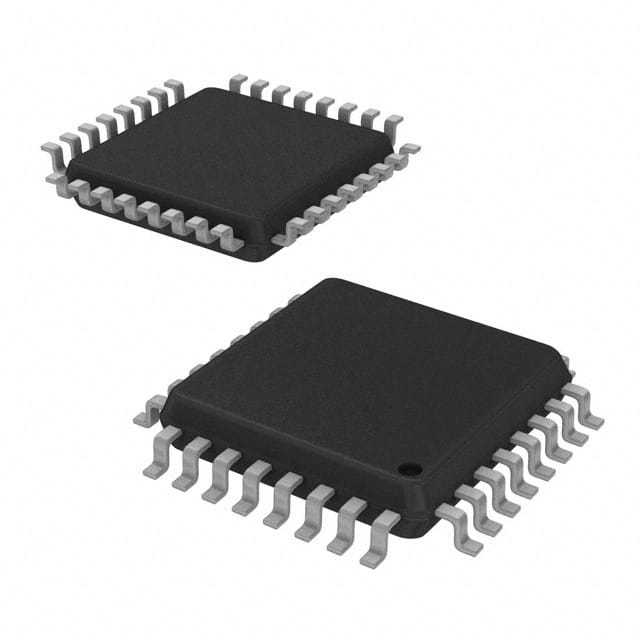
- Package: QFN-16
- Essence: High-speed data transmission and noise reduction
- Packaging/Quantity: Tape & Reel, 2500 pieces per reel
Specifications and Parameters
- Supply Voltage Range: 3.0V to 3.6V
- Operating Temperature Range: -40°C to +85°C
- Input Voltage Range: 0V to VCC
- Output Voltage Range: 0V to VCC
- Maximum Data Rate: 1.5 Gbps
- Propagation Delay: 200 ps (typical)
Detailed and Complete Pin Configuration
- VCC
- GND
- IN0P
- IN0N
- OUT0P
- OUT0N
- IN1P
- IN1N
- OUT1P
- OUT1N
- IN2P
- IN2N
- OUT2P
- OUT2N
- NC
- NC
Functional Characteristics
- LVDS input and output compatibility
- High-speed data transmission up to 1.5 Gbps
- Low power consumption
- Wide operating temperature range
- ESD protection on all pins
Advantages and Disadvantages
Advantages: - High-speed data transmission capability - Low power consumption - Wide operating temperature range - ESD protection for enhanced reliability
Disadvantages: - Limited number of input/output channels - Not suitable for applications requiring higher data rates
Applicable Range of Products
- Communication systems
- Data transmission equipment
- Industrial automation
- Medical devices
- Test and measurement instruments
Working Principles
NB4L6254FAR2G is designed to condition and shift the levels of LVDS signals. It receives LVDS input signals, amplifies them, and provides LVDS output signals with improved noise immunity and reduced signal degradation.
Detailed Application Field Plans
- Communication Systems: Used for high-speed data transmission between network equipment.
- Data Transmission Equipment: Enables reliable data transfer in high-speed interfaces such as USB, HDMI, and DisplayPort.
- Industrial Automation: Facilitates communication between control systems and sensors/actuators.
- Medical Devices: Ensures accurate and noise-free signal transmission in medical imaging and diagnostic equipment.
- Test and Measurement Instruments: Provides precise signal conditioning for accurate measurements in electronic testing.
Detailed Alternative Models
- NB4N111K: Quad Differential Line Receiver
- NB7VQ1006M: 2.5 V / 3.3 V Differential Receiver
- NB3N551: Low Skew Clock Buffer
- NB6L11SMNG: Differential PECL/LVPECL Clock Fanout Buffer
- NB3N2304: 3.3 V Dual Differential Clock Fanout Buffer
5 Common Technical Questions and Answers
Q: What is the maximum data rate supported by NB4L6254FAR2G? A: The maximum data rate is 1.5 Gbps.
Q: Can NB4L6254FAR2G operate at temperatures below freezing? A: Yes, it can operate within a temperature range of -40°C to +85°C.
Q: Does NB4L6254FAR2G provide ESD protection on all pins? A: Yes, it offers ESD protection on all pins for enhanced reliability.
Q: What is the package type of NB4L6254FAR2G? A: It comes in a QFN-16 package.
Q: Is NB4L6254FAR2G suitable for applications requiring high-speed data transmission? A: Yes, it is designed for high-speed data transmission up to 1.5 Gbps.