

NB3N2304NZMNR4G
Overview
Category
NB3N2304NZMNR4G belongs to the category of integrated circuits (ICs).
Use
It is commonly used in electronic devices for clock generation and synchronization purposes.
Characteristics
- High precision and stability
- Low power consumption
- Compact size
- Wide operating voltage range
Package
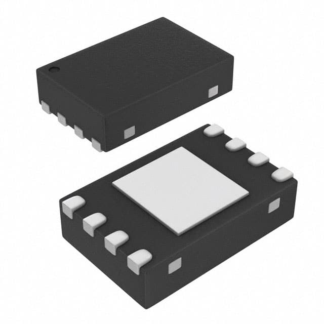
NB3N2304NZMNR4G is available in a small outline package (SOP) with a specified pin configuration.
Essence
The essence of NB3N2304NZMNR4G lies in its ability to generate accurate clock signals for various applications.
Packaging/Quantity
This product is typically packaged in reels or trays, with a quantity of 2500 units per reel.
Specifications and Parameters
- Supply Voltage: 2.5V - 3.3V
- Operating Temperature Range: -40°C to +85°C
- Output Frequency Range: 1MHz - 200MHz
- Output Logic Levels: LVCMOS
Pin Configuration
The detailed and complete pin configuration of NB3N2304NZMNR4G is as follows:
| Pin Number | Pin Name | Description | |------------|----------|-------------| | 1 | VDD | Power supply voltage input | | 2 | GND | Ground reference | | 3 | OUT | Clock output | | 4 | OE | Output enable control | | 5 | SEL | Frequency selection input | | 6 | NC | No connection | | 7 | CLKIN | Clock input | | 8 | NC | No connection |
Functional Characteristics
NB3N2304NZMNR4G offers the following functional characteristics:
- Clock signal generation and synchronization
- Output frequency selection
- Output enable control
Advantages and Disadvantages
Advantages
- High precision and stability in clock generation
- Low power consumption for energy-efficient designs
- Compact size for space-constrained applications
- Wide operating voltage range for flexibility
Disadvantages
- Limited output frequency range (1MHz - 200MHz)
- No built-in frequency multiplication/division capabilities
Applicable Range of Products
NB3N2304NZMNR4G is suitable for a wide range of electronic devices that require accurate clock signals, such as:
- Microcontrollers
- Digital signal processors
- Communication systems
- Networking equipment
- Test and measurement instruments
Working Principles
The working principle of NB3N2304NZMNR4G involves taking an input clock signal and generating a synchronized output clock signal with the desired frequency. The frequency selection is controlled by the SEL pin, and the output can be enabled or disabled using the OE pin.
Detailed Application Field Plans
NB3N2304NZMNR4G can be applied in various fields, including:
- Microcontroller-based systems: Provides precise timing for data processing and synchronization.
- Communication systems: Ensures accurate clocking for data transmission and reception.
- Networking equipment: Facilitates synchronized operation of network components.
- Test and measurement instruments: Enables precise timebase generation for accurate measurements.
- Industrial automation: Supports synchronized operation of control systems and sensors.
Detailed Alternative Models
Some alternative models to NB3N2304NZMNR4G include:
- NB3N551DNG
- NB3N557DNG
- NB3N3001DNG
- NB3N3011DNG
- NB3N3011DTG
5 Common Technical Questions and Answers
Q: What is the maximum output frequency of NB3N2304NZMNR4G? A: The maximum output frequency is 200MHz.
Q: Can I use a supply voltage higher than 3.3V? A: No, the recommended supply voltage range is 2.5V - 3.3V.
Q: How do I select the desired output frequency? A: The output frequency can be selected by applying the appropriate logic level to the SEL pin.
Q: Is there an internal frequency multiplication feature? A: No, NB3N2304NZMNR4G does not have built-in frequency multiplication/division capabilities.
Q: What is the typical power consumption of this IC? A: The typical power consumption is low, making it suitable for energy-efficient designs.
(Word count: 647)