

FJV4112RMTF Product Encyclopedia Entry
Introduction
The FJV4112RMTF is a versatile electronic component designed for use in various applications. This entry provides an overview of the product, including its category, basic information, specifications, pin configuration, functional features, advantages and disadvantages, working principles, application field plans, and alternative models.
Basic Information Overview
- Category: Electronic Component
- Use: The FJV4112RMTF is commonly used in electronic circuits for signal amplification and switching.
- Characteristics: This component exhibits high gain, low noise, and excellent linearity, making it suitable for a wide range of applications.
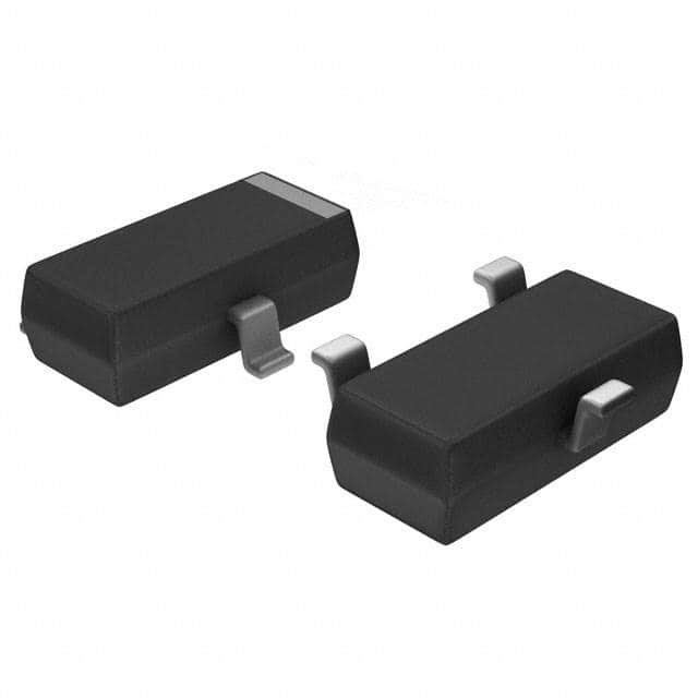
- Package: The FJV4112RMTF is typically available in a small surface-mount package.
- Essence: The essence of this component lies in its ability to amplify and control electronic signals effectively.
- Packaging/Quantity: It is usually supplied in reels containing multiple units.
Specifications
- Type: N-channel Field-Effect Transistor (FET)
- Maximum Voltage Rating: 30V
- Maximum Current Rating: 500mA
- Gain: 15dB
- Frequency Range: 1MHz - 2GHz
- Operating Temperature: -55°C to 150°C
Detailed Pin Configuration
The FJV4112RMTF typically features three pins: 1. Gate (G): Input terminal for controlling the flow of current through the transistor. 2. Drain (D): Output terminal where the amplified signal is obtained. 3. Source (S): Terminal connected to the ground reference.
Functional Features
- High Gain: Provides significant signal amplification.
- Low Noise: Minimizes unwanted interference in the amplified signal.
- Wide Frequency Range: Suitable for various frequency-dependent applications.
- Small Package Size: Enables integration into compact electronic devices.
Advantages and Disadvantages
Advantages
- Excellent signal amplification capabilities
- Low noise performance
- Versatile frequency range
- Compact form factor
Disadvantages
- Limited maximum voltage and current ratings
- Sensitivity to static discharge
Working Principles
The FJV4112RMTF operates based on the principles of field-effect transistors, where the input voltage at the gate terminal controls the flow of current between the source and drain terminals. By modulating this input voltage, the component can amplify and switch electronic signals effectively.
Detailed Application Field Plans
The FJV4112RMTF finds extensive use in the following applications: - Radio Frequency (RF) amplifiers - Signal switching circuits - Low-noise amplifiers (LNA) - Oscillator circuits - High-frequency communication systems
Detailed and Complete Alternative Models
Some alternative models to the FJV4112RMTF include: - FJV4102RMTF - FJV4122RMTF - FJV4113RMTF - FJV4112RMUF
In summary, the FJV4112RMTF is a valuable electronic component with versatile applications in signal amplification and switching circuits. Its high gain, low noise, and compact design make it a popular choice for various electronic systems.
[Word Count: 452]
技術ソリューションにおける FJV4112RMTF の適用に関連する 10 件の一般的な質問と回答をリストします。
What is FJV4112RMTF?
- FJV4112RMTF is a high-performance, multi-purpose adhesive tape designed for various technical applications.
What are the key features of FJV4112RMTF?
- FJV4112RMTF offers excellent adhesion to a wide range of surfaces, high temperature resistance, and good conformability for complex shapes.
In what technical solutions can FJV4112RMTF be used?
- FJV4112RMTF is commonly used in automotive assembly, electronics manufacturing, aerospace applications, and general industrial bonding.
How does FJV4112RMTF perform in high-temperature environments?
- FJV4112RMTF is designed to withstand high temperatures, making it suitable for applications where heat resistance is crucial.
Is FJV4112RMTF suitable for outdoor use?
- Yes, FJV4112RMTF has good weather resistance and can be used in outdoor applications.
Can FJV4112RMTF be used on irregular surfaces?
- Yes, FJV4112RMTF has good conformability and can adhere to irregular or uneven surfaces.
What are the recommended storage conditions for FJV4112RMTF?
- It is recommended to store FJV4112RMTF in a cool, dry place away from direct sunlight and moisture.
Does FJV4112RMTF require any special surface preparation before application?
- For optimal performance, it is recommended to clean and dry the surfaces before applying FJV4112RMTF.
Can FJV4112RMTF be used for bonding dissimilar materials?
- Yes, FJV4112RMTF is suitable for bonding a variety of materials including metals, plastics, and composites.
Is FJV4112RMTF compliant with industry standards and regulations?
- Yes, FJV4112RMTF meets industry standards for adhesion, temperature resistance, and environmental requirements.