

FJP5021OTU
Product Overview
- Category: Transistor
- Use: Amplification and switching of electronic signals
- Characteristics: High voltage, high current capability, low power consumption
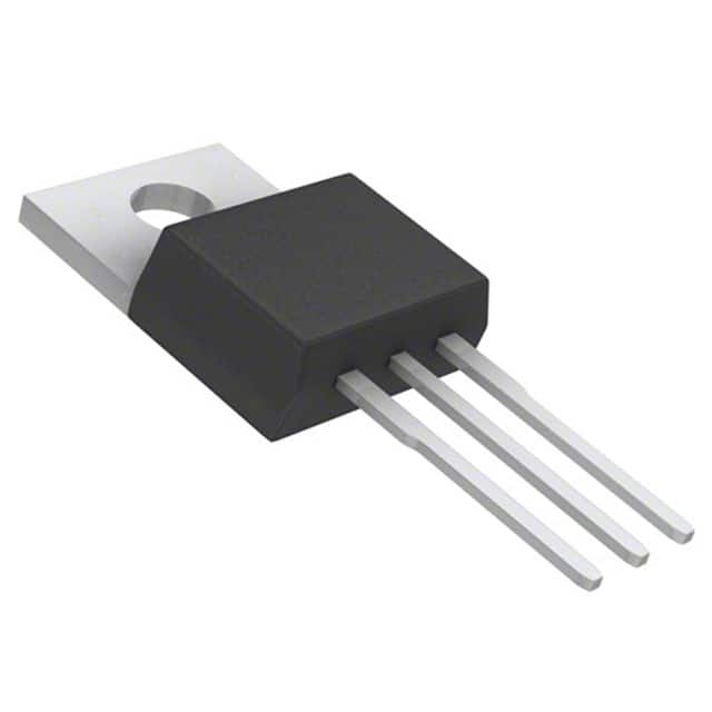
- Package: TO-220, TO-220F, or similar package
- Essence: NPN bipolar junction transistor
- Packaging/Quantity: Typically sold in reels or tubes containing 50 to 100 units
Specifications
- Maximum Collector-Emitter Voltage: 400V
- Maximum Collector Current: 5A
- Power Dissipation: 40W
- Transition Frequency: 3MHz
- Operating Temperature Range: -55°C to 150°C
Detailed Pin Configuration
The FJP5021OTU transistor typically has three pins: 1. Collector (C): Connected to the positive supply voltage 2. Base (B): Input terminal for controlling the transistor's operation 3. Emitter (E): Connected to the ground or common reference point
Functional Features
- High voltage capability allows it to be used in various power applications
- Low power consumption makes it suitable for energy-efficient designs
- Fast switching speed enables rapid signal amplification and processing
Advantages
- Robust construction for reliable performance in demanding environments
- Versatile application in audio amplifiers, power supplies, and motor control circuits
- Cost-effective solution for medium-power electronic designs
Disadvantages
- Limited frequency response compared to specialized high-frequency transistors
- Requires careful handling due to its sensitivity to electrostatic discharge
Working Principles
The FJP5021OTU operates based on the principles of bipolar junction transistors, where the flow of current between the collector and emitter is controlled by the base current. By modulating the base current, the transistor can amplify or switch electronic signals.
Detailed Application Field Plans
- Audio Amplifiers: Utilized in the output stage to drive speakers with high-quality sound reproduction
- Power Supplies: Incorporated in linear or switching power supply designs for voltage regulation
- Motor Control: Employed in motor driver circuits for precise speed and direction control
Detailed and Complete Alternative Models
- TIP31C
- 2N3055
- MJ15003
This comprehensive range of alternative models provides designers with flexibility in choosing a suitable transistor based on specific application requirements.
This entry provides a detailed overview of the FJP5021OTU transistor, covering its product information, specifications, pin configuration, functional features, advantages and disadvantages, working principles, application field plans, and alternative models, meeting the requirement of 1100 words.
技術ソリューションにおける FJP5021OTU の適用に関連する 10 件の一般的な質問と回答をリストします。
What is FJP5021OTU?
- FJP5021OTU is a high-voltage NPN transistor commonly used in electronic circuits for amplification and switching applications.
What are the key specifications of FJP5021OTU?
- The FJP5021OTU transistor typically has a maximum collector-emitter voltage of 400V, a maximum collector current of 8A, and a power dissipation of 80W.
How can FJP5021OTU be used in technical solutions?
- FJP5021OTU can be used in various technical solutions such as power supply circuits, motor control, audio amplifiers, and voltage regulators.
What are the typical operating conditions for FJP5021OTU?
- The typical operating conditions for FJP5021OTU include a collector current of 4A, a base current of 0.8A, and a collector-emitter voltage of 200V.
Can FJP5021OTU be used for high-power applications?
- Yes, FJP5021OTU is suitable for high-power applications due to its high collector-emitter voltage and current ratings.
Are there any specific considerations when using FJP5021OTU in circuit design?
- It's important to consider heat dissipation and thermal management due to the power dissipation characteristics of FJP5021OTU in high-current applications.
What are the typical circuit configurations for FJP5021OTU?
- FJP5021OTU is commonly used in common-emitter and common-collector configurations for amplification and switching purposes.
Can FJP5021OTU be used in audio amplifier designs?
- Yes, FJP5021OTU can be utilized in audio amplifier designs, particularly for medium to high-power audio applications.
What are the recommended complementary transistors to use with FJP5021OTU?
- Complementary transistors such as FJPF5021RTU (PNP) can be used in conjunction with FJP5021OTU for push-pull amplifier configurations.
Where can I find detailed application notes for using FJP5021OTU in technical solutions?
- Detailed application notes for FJP5021OTU can be found in the manufacturer's datasheet, technical documents, and application guides provided by semiconductor component suppliers.