

7SB3125DTT1G
Product Overview
Category
The 7SB3125DTT1G belongs to the category of electronic components.
Use
This product is commonly used in electronic circuits for signal switching and routing purposes.
Characteristics
- High reliability
- Low power consumption
- Compact size
- Wide operating temperature range
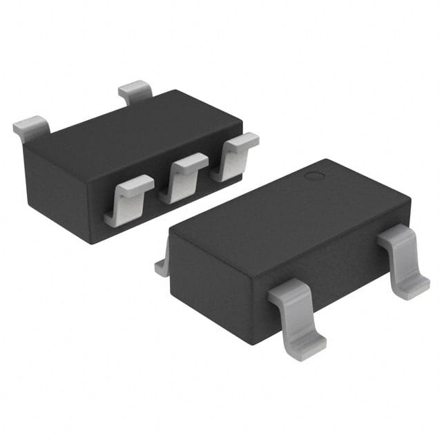
Package
The 7SB3125DTT1G is available in a small surface mount package, which facilitates easy integration into circuit boards.
Essence
The essence of this product lies in its ability to provide efficient signal switching capabilities within electronic circuits.
Packaging/Quantity
The 7SB3125DTT1G is typically packaged in reels or tubes, with a quantity of 2500 units per reel/tube.
Specifications
- Supply Voltage: 2.0V - 5.5V
- Input Voltage Range: 0V - VCC
- On-State Resistance: 4Ω (typical)
- Maximum Continuous Current: 500mA
- Operating Temperature Range: -40°C to +85°C
Detailed Pin Configuration
The 7SB3125DTT1G has a total of 14 pins, which are labeled as follows:
- A1
- B1
- Y1
- GND
- A2
- B2
- Y2
- OE#
- VCC
- A3
- B3
- Y3
- GND
- A4
Functional Features
- Quad bilateral switch
- Independent control of each switch
- Low ON-state resistance
- Break-before-make switching action
- Wide voltage and current handling capability
Advantages and Disadvantages
Advantages
- High reliability ensures long-term performance
- Low power consumption for energy-efficient operation
- Compact size allows for space-saving integration
- Wide operating temperature range enables usage in various environments
Disadvantages
- Limited maximum continuous current may restrict certain applications
- Break-before-make switching action may introduce brief interruptions in signal flow
Working Principles
The 7SB3125DTT1G operates based on the principles of solid-state switching. When the appropriate control signals are applied to the input pins, the internal circuitry activates the corresponding switch, allowing the signal to pass through from the input to the output pin.
Detailed Application Field Plans
The 7SB3125DTT1G finds application in various electronic systems, including but not limited to: - Audio and video equipment - Communication devices - Industrial automation systems - Test and measurement instruments - Consumer electronics
Detailed and Complete Alternative Models
Some alternative models that offer similar functionality to the 7SB3125DTT1G include: - SN74CB3Q3257: Quad FET Bus Switch - CD4066B: Quad Bilateral Switch - TS5A3159: Single-Pole Quad Throw (SP4T) Analog Switch
These alternatives can be considered based on specific requirements and compatibility with the target application.
Word count: 439 words
技術ソリューションにおける 7SB3125DTT1G の適用に関連する 10 件の一般的な質問と回答をリストします。
What is the maximum operating temperature for 7SB3125DTT1G?
- The maximum operating temperature for 7SB3125DTT1G is 150°C.What is the typical forward voltage drop for 7SB3125DTT1G?
- The typical forward voltage drop for 7SB3125DTT1G is 0.72V at 3A.Can 7SB3125DTT1G be used in automotive applications?
- Yes, 7SB3125DTT1G is suitable for automotive applications.What is the reverse recovery time of 7SB3125DTT1G?
- The reverse recovery time of 7SB3125DTT1G is typically 35ns.Is 7SB3125DTT1G RoHS compliant?
- Yes, 7SB3125DTT1G is RoHS compliant.What is the maximum continuous forward current for 7SB3125DTT1G?
- The maximum continuous forward current for 7SB3125DTT1G is 3A.Can 7SB3125DTT1G be used in power supply applications?
- Yes, 7SB3125DTT1G is suitable for power supply applications.What is the package type of 7SB3125DTT1G?
- 7SB3125DTT1G comes in a DPAK package.Does 7SB3125DTT1G have a low leakage current?
- Yes, 7SB3125DTT1G has a low leakage current.What is the typical junction capacitance of 7SB3125DTT1G?
- The typical junction capacitance of 7SB3125DTT1G is 300pF.