

Encyclopedia Entry: 74AUP1G58FHX
Product Overview
Category
The 74AUP1G58FHX belongs to the category of integrated circuits (ICs) and specifically falls under the family of logic gates.
Use
This product is primarily used for logical operations in digital electronic circuits. It serves as a single-input AND gate, allowing for the manipulation of binary data.
Characteristics
- Single-input AND gate
- Low power consumption
- High-speed operation
- Wide operating voltage range
- Small package size
- RoHS compliant
Package
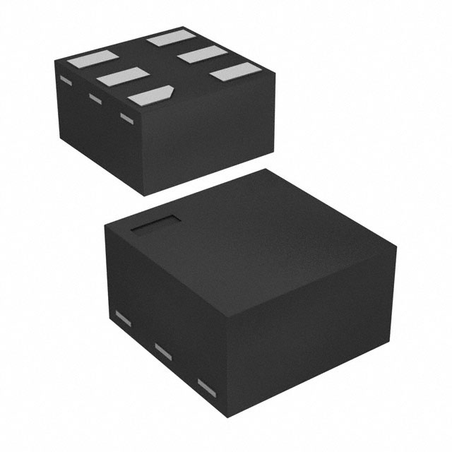
The 74AUP1G58FHX is available in a small form factor package, such as SOT353 or XSON6. These packages offer compactness and ease of integration into various electronic devices.
Essence
The essence of the 74AUP1G58FHX lies in its ability to perform logical AND operations on a single input signal, providing an output based on the input's binary state.
Packaging/Quantity
The product is typically supplied in reels or tubes, with quantities varying depending on the manufacturer and distributor. Common quantities include 3000 or 5000 units per reel.
Specifications
- Supply Voltage Range: 0.8V to 3.6V
- Input Voltage Range: 0V to VCC
- Output Voltage Range: 0V to VCC
- Operating Temperature Range: -40°C to +85°C
- Propagation Delay: <5ns
- Maximum Quiescent Current: 10μA
Detailed Pin Configuration
The 74AUP1G58FHX features a simple pin configuration:
____
   A --|    |-- VCC
       |    |
 GND --|____|-- Y
- A: Input pin
- VCC: Power supply pin
- GND: Ground pin
- Y: Output pin
Functional Features
The key functional features of the 74AUP1G58FHX include:
- Single-input AND gate operation
- Fast propagation delay for high-speed applications
- Wide operating voltage range allows compatibility with various systems
- Low power consumption for energy-efficient designs
- RoHS compliance ensures environmental friendliness
Advantages and Disadvantages
Advantages
- Compact package size enables space-saving designs
- Low power consumption prolongs battery life in portable devices
- High-speed operation facilitates efficient data processing
- Wide operating voltage range enhances versatility in different applications
Disadvantages
- Limited to single-input AND gate functionality, limiting its use in more complex logic operations
- May not be suitable for applications requiring multiple input gates or specialized functions
Working Principles
The 74AUP1G58FHX operates based on the principles of digital logic. When a logical HIGH (1) signal is applied to the input pin (A), the output pin (Y) will produce a logical HIGH (1). Conversely, when a logical LOW (0) signal is applied to the input pin (A), the output pin (Y) will produce a logical LOW (0).
Detailed Application Field Plans
The 74AUP1G58FHX finds application in various fields, including but not limited to:
Consumer Electronics:
- Mobile phones
- Tablets
- Digital cameras
Automotive:
- Infotainment systems
- Advanced driver-assistance systems (ADAS)
- Lighting control
Industrial Automation:
- Programmable logic controllers (PLCs)
- Motor control
- Sensor interfacing
Internet of Things (IoT):
- Smart home devices
- Wearable technology
- Environmental monitoring systems
Detailed and Complete Alternative Models
Some alternative models that offer similar functionality to the 74AUP1G58FHX include:
- SN74LVC1G58DBVR (Texas Instruments)
- MC74VHC1G58DTT1G (ON Semiconductor)
- NC7SZ58P6X (Fairchild Semiconductor)
These alternatives can be considered based on specific requirements, availability, and compatibility with existing designs.
In conclusion, the 74AUP1G58FHX is a single-input AND gate integrated circuit that offers high-speed operation, low power consumption, and wide operating voltage range. Its compact package size and RoHS compliance make it suitable for various applications in consumer electronics, automotive, industrial automation, and IoT. While it has limitations in terms of its single-input functionality, alternative models are available to cater to different design needs.
技術ソリューションにおける 74AUP1G58FHX の適用に関連する 10 件の一般的な質問と回答をリストします。
Sure! Here are 10 common questions and answers related to the application of 74AUP1G58FHX in technical solutions:
Q1: What is the 74AUP1G58FHX? A1: The 74AUP1G58FHX is a single configurable multiple function gate, specifically a configurable AND/OR gate, designed for use in various digital logic applications.
Q2: What is the operating voltage range of the 74AUP1G58FHX? A2: The 74AUP1G58FHX operates within a voltage range of 0.8V to 3.6V.
Q3: What is the maximum output current of the 74AUP1G58FHX? A3: The maximum output current of the 74AUP1G58FHX is typically around 32mA.
Q4: Can the 74AUP1G58FHX be used as an AND gate? A4: Yes, the 74AUP1G58FHX can be configured as an AND gate by connecting its inputs and configuring the control pin accordingly.
Q5: Can the 74AUP1G58FHX be used as an OR gate? A5: Yes, the 74AUP1G58FHX can be configured as an OR gate by connecting its inputs and configuring the control pin accordingly.
Q6: What is the propagation delay of the 74AUP1G58FHX? A6: The propagation delay of the 74AUP1G58FHX is typically around 2.5ns.
Q7: Can the 74AUP1G58FHX be used in high-speed applications? A7: Yes, the 74AUP1G58FHX is designed for high-speed operation and can be used in applications that require fast switching times.
Q8: Is the 74AUP1G58FHX compatible with other logic families? A8: Yes, the 74AUP1G58FHX is compatible with a wide range of logic families, including CMOS, TTL, and LVCMOS.
Q9: Can the 74AUP1G58FHX be used in battery-powered devices? A9: Yes, the 74AUP1G58FHX operates within a low voltage range and has low power consumption, making it suitable for battery-powered devices.
Q10: What package options are available for the 74AUP1G58FHX? A10: The 74AUP1G58FHX is available in various package options, such as SOT353, XSON6, and DFN6.