

PMBFJ110,215
Product Overview
Category
The PMBFJ110,215 belongs to the category of field-effect transistors (FETs).
Use
It is commonly used as a switching device in electronic circuits.
Characteristics
- Low power loss
- High efficiency
- Fast switching speed
Package
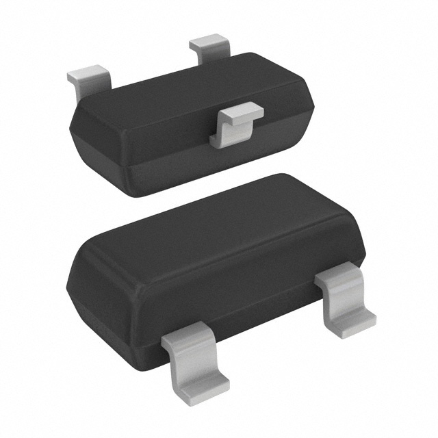
The PMBFJ110,215 is typically available in a SOT-23 package.
Essence
This transistor is essential for controlling the flow of current in electronic devices.
Packaging/Quantity
It is usually packaged in reels with quantities varying based on manufacturer specifications.
Specifications
- Drain-Source Voltage (VDS): 40V
- Continuous Drain Current (ID): 0.2A
- Total Power Dissipation: 250mW
- Gate-Source Voltage (VGS): ±20V
- Operating and Storage Temperature Range: -55°C to +150°C
Detailed Pin Configuration
The PMBFJ110,215 has three pins: 1. Source (S) 2. Gate (G) 3. Drain (D)
Functional Features
- Low input and output capacitance
- High input impedance
- Enhanced thermal performance
Advantages
- Small form factor
- Low power consumption
- Reliable switching performance
Disadvantages
- Limited maximum voltage and current ratings
- Sensitivity to electrostatic discharge
Working Principles
The PMBFJ110,215 operates based on the field effect controlled by the voltage applied to the gate terminal, allowing or restricting the flow of current between the source and drain terminals.
Detailed Application Field Plans
The PMBFJ110,215 is widely used in: - Portable electronic devices - Battery management systems - Switching power supplies - LED lighting applications
Detailed and Complete Alternative Models
- PMBFJ109,215
- PMBFJ108,215
- PMBFJ111,215
In conclusion, the PMBFJ110,215 is a versatile field-effect transistor with a compact design and efficient performance, making it suitable for various low-power electronic applications.
Word Count: 280
技術ソリューションにおける PMBFJ110,215 の適用に関連する 10 件の一般的な質問と回答をリストします。
Sure, here are 10 common questions and answers related to the application of PMBFJ110,215 in technical solutions:
What is PMBFJ110,215?
- PMBFJ110,215 is a field-effect transistor (FET) designed for high-speed switching applications.
What are the key features of PMBFJ110,215?
- PMBFJ110,215 features low capacitance, low on-state resistance, and fast switching speed, making it suitable for high-frequency applications.
What are the typical applications of PMBFJ110,215?
- PMBFJ110,215 is commonly used in RF amplifiers, oscillators, mixers, and other high-frequency circuits.
What is the maximum voltage and current rating for PMBFJ110,215?
- The maximum voltage rating is typically around 25V, and the maximum continuous drain current is around 50mA.
How do I properly bias PMBFJ110,215 in my circuit?
- PMBFJ110,215 is typically biased using a DC voltage source to set the desired operating point for the transistor.
Can PMBFJ110,215 be used in low-noise amplifier (LNA) designs?
- Yes, PMBFJ110,215's low noise figure and high gain make it suitable for use in LNA designs.
What are the thermal considerations for using PMBFJ110,215 in high-power applications?
- In high-power applications, proper heat sinking and thermal management should be considered to ensure the FET operates within its temperature limits.
Are there any specific layout considerations when using PMBFJ110,215 in a PCB design?
- It's important to minimize parasitic capacitances and inductances in the layout to maintain the high-frequency performance of PMBFJ110,215.
Can PMBFJ110,215 be used in battery-powered devices?
- Yes, PMBFJ110,215's low power consumption and high efficiency make it suitable for battery-powered devices.
Where can I find detailed application notes and reference designs for PMBFJ110,215?
- Application notes and reference designs for PMBFJ110,215 can typically be found on the manufacturer's website or in technical literature related to RF and high-frequency circuit design.