

PCA9671DB,112
Product Overview
Category: Integrated Circuit (IC)
Use: The PCA9671DB,112 is a versatile 8-bit I2C-bus and SMBus I/O expander designed for general-purpose input/output expansion applications. It provides an easy way to increase the number of I/O pins available in a microcontroller-based system.
Characteristics: - 8-bit bidirectional I/O port - I2C-bus and SMBus compatible - Low standby current consumption - Schmitt trigger action on all inputs - Noise filter on SCL/SDA inputs - Internal power-on reset - Active LOW reset input - 5 V tolerant inputs - Open-drain interrupt output - Address by three hardware address pins - 400 kHz Fast-mode I2C-bus - ESD protection exceeds 2000 V HBM per JESD22-A114, 200 V MM per JESD22-A115, and 1000 V CDM per JESD22-C101
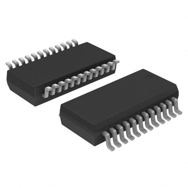
Package: The PCA9671DB,112 comes in a small outline package (SO) with 16 pins.
Essence: The essence of PCA9671DB,112 lies in its ability to expand the number of I/O pins in a microcontroller-based system, providing flexibility and increased functionality.
Packaging/Quantity: The PCA9671DB,112 is typically sold in reels or tubes, with a quantity of 2500 units per reel/tube.
Specifications
- Supply voltage range: 2.3 V to 5.5 V
- Operating temperature range: -40°C to +85°C
- I/O voltage level: 0 V to VDD
- Standby current: 1 μA (typical)
- Output current: ±10 mA
- Input leakage current: ±1 μA
Pin Configuration
The PCA9671DB,112 has a total of 16 pins. The pin configuration is as follows:
```
| | | 1 2 3 | |_____________| | | | 4 5 6 | |_____________| | | | 7 8 9 | |_____________| | | | 10 11 12 | |_____________| ```
Pin Description: 1. SDA - Serial Data Line 2. SCL - Serial Clock Line 3. INT - Interrupt Output 4. A0 - Hardware Address Bit 0 5. A1 - Hardware Address Bit 1 6. A2 - Hardware Address Bit 2 7. GND - Ground 8. P0 - I/O Port 0 9. P1 - I/O Port 1 10. P2 - I/O Port 2 11. P3 - I/O Port 3 12. P4 - I/O Port 4
Functional Features
- Bidirectional I/O expansion: The PCA9671DB,112 provides 8-bit bidirectional I/O port, allowing for easy expansion of I/O pins in a microcontroller-based system.
- I2C-bus and SMBus compatibility: It is compatible with both I2C-bus and SMBus protocols, ensuring seamless integration into existing systems.
- Low standby current consumption: The device consumes very low standby current, making it suitable for battery-powered applications.
- Schmitt trigger action: All inputs feature Schmitt trigger action, providing noise immunity and improved signal integrity.
- Noise filter: The SCL/SDA inputs are equipped with a noise filter, further enhancing the reliability of communication.
- Power-on reset: The PCA9671DB,112 has an internal power-on reset circuitry that ensures proper initialization upon power-up.
- Reset input: An active LOW reset input allows for external reset control.
- 5 V tolerant inputs: The device supports 5 V tolerant inputs, enabling compatibility with both 3.3 V and 5 V systems.
- Open-drain interrupt output: The interrupt output is open-drain, allowing for easy integration with other devices.
- Addressing flexibility: The device can be addressed using three hardware address pins (A0, A1, A2), providing flexibility in system configuration.
- Fast-mode I2C-bus: It supports a fast-mode I2C-bus with a maximum frequency of 400 kHz.
- ESD protection: The PCA9671DB,112 offers robust ESD protection, exceeding industry standards.
Advantages and Disadvantages
Advantages: - Easy expansion of I/O pins - Compatibility with I2C-bus and SMBus protocols - Low standby current consumption - Noise
技術ソリューションにおける PCA9671DB,112 の適用に関連する 10 件の一般的な質問と回答をリストします。
Sure! Here are 10 common questions and answers related to the application of PCA9671DB,112 in technical solutions:
Q1: What is PCA9671DB,112? A1: PCA9671DB,112 is a general-purpose I/O expander that provides remote I/O expansion for most microcontroller families via the I2C-bus interface.
Q2: What is the maximum number of I/O pins supported by PCA9671DB,112? A2: PCA9671DB,112 supports up to 16 I/O pins.
Q3: How can I communicate with PCA9671DB,112? A3: PCA9671DB,112 uses the I2C-bus interface for communication with the microcontroller.
Q4: Can PCA9671DB,112 be used with both 3.3V and 5V microcontrollers? A4: Yes, PCA9671DB,112 is compatible with both 3.3V and 5V microcontrollers.
Q5: What is the maximum frequency supported by PCA9671DB,112? A5: PCA9671DB,112 supports a maximum frequency of 400 kHz.
Q6: Can PCA9671DB,112 be used for both input and output operations? A6: Yes, PCA9671DB,112 can be configured as either an input or output device on a per-pin basis.
Q7: Is PCA9671DB,112 capable of driving LEDs directly? A7: Yes, PCA9671DB,112 can source and sink current, making it suitable for driving LEDs directly.
Q8: Can PCA9671DB,112 be cascaded with other I/O expanders? A8: Yes, multiple PCA9671DB,112 devices can be cascaded together to expand the number of I/O pins.
Q9: Does PCA9671DB,112 have built-in pull-up resistors? A9: Yes, PCA9671DB,112 has programmable internal pull-up resistors for each I/O pin.
Q10: What is the operating voltage range of PCA9671DB,112? A10: PCA9671DB,112 operates within a voltage range of 2.3V to 5.5V.
Please note that these answers are general and may vary depending on the specific implementation and configuration of PCA9671DB,112 in your technical solution.