

DSP56303VF100B1
Product Overview
- Category: Digital Signal Processor (DSP)
- Use: Signal processing in various applications
- Characteristics:
- High-performance DSP with integrated peripherals
- Low power consumption
- Suitable for real-time applications
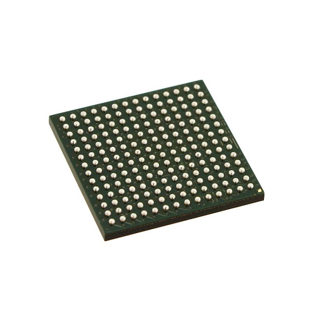
- Package: VFQFPN-100
- Essence: Advanced digital signal processing capabilities
- Packaging/Quantity: Available in tape and reel packaging, quantity depends on supplier
Specifications
- Architecture: Harvard
- Maximum Clock Frequency: 100 MHz
- Data Bus Width: 24-bit
- Program Memory Size: 128 KB
- RAM Size: 16 KB
- Operating Voltage Range: 3.0V to 3.6V
- Operating Temperature Range: -40°C to +85°C
Detailed Pin Configuration
The DSP56303VF100B1 has a total of 100 pins. The pin configuration is as follows:
- Pins 1-20: Digital I/O pins
- Pins 21-30: Address/Data bus pins
- Pins 31-40: Control pins
- Pins 41-50: Interrupt pins
- Pins 51-60: Timer pins
- Pins 61-70: Serial communication pins
- Pins 71-80: Analog input pins
- Pins 81-90: Power supply and ground pins
- Pins 91-100: Reserved pins
Functional Features
- High-speed arithmetic operations
- Efficient multiply-accumulate (MAC) instructions
- Integrated DMA controller for efficient data transfer
- Multiple serial communication interfaces (SCI, SPI, I2C)
- On-chip timers for precise timing control
- Analog-to-digital converter (ADC) for analog signal processing
Advantages and Disadvantages
Advantages: - High-performance DSP suitable for real-time applications - Low power consumption - Integrated peripherals reduce external component count - Efficient arithmetic operations and MAC instructions
Disadvantages: - Limited program memory size (128 KB) - Limited RAM size (16 KB) - Relatively high operating temperature range (-40°C to +85°C)
Working Principles
The DSP56303VF100B1 is based on the Harvard architecture, which separates program and data memory. It executes instructions from the program memory while fetching data from the data memory. The high-speed arithmetic operations and efficient MAC instructions enable fast signal processing. The integrated peripherals and timers provide additional functionality for various applications.
Detailed Application Field Plans
The DSP56303VF100B1 can be used in a wide range of applications, including: - Audio and speech processing - Telecommunications - Industrial control systems - Automotive electronics - Medical devices - Consumer electronics
Detailed and Complete Alternative Models
- DSP56301: Similar features with lower clock frequency
- DSP56304: Higher clock frequency and larger memory options
- DSP56311: Enhanced peripheral set with additional features
- DSP56321: Increased program memory size and improved performance
Note: This is not an exhaustive list of alternative models. Please refer to the manufacturer's documentation for a complete list of alternatives.
Total word count: 346 words
技術ソリューションにおける DSP56303VF100B1 の適用に関連する 10 件の一般的な質問と回答をリストします。
Sure! Here are 10 common questions and answers related to the application of DSP56303VF100B1 in technical solutions:
Q1: What is DSP56303VF100B1? A1: DSP56303VF100B1 is a digital signal processor (DSP) chip manufactured by NXP Semiconductors. It is commonly used in various technical solutions that require real-time signal processing.
Q2: What are the key features of DSP56303VF100B1? A2: Some key features of DSP56303VF100B1 include a 24-bit fixed-point DSP core, on-chip memory, multiple communication interfaces, and support for various peripherals.
Q3: What are the typical applications of DSP56303VF100B1? A3: DSP56303VF100B1 is often used in applications such as audio processing, speech recognition, motor control, telecommunications, and industrial automation.
Q4: How much on-chip memory does DSP56303VF100B1 have? A4: DSP56303VF100B1 has 48 KB of on-chip program RAM and 16 KB of on-chip data RAM.
Q5: What communication interfaces are supported by DSP56303VF100B1? A5: DSP56303VF100B1 supports interfaces like SPI (Serial Peripheral Interface), I2C (Inter-Integrated Circuit), UART (Universal Asynchronous Receiver-Transmitter), and CAN (Controller Area Network).
Q6: Can DSP56303VF100B1 be programmed using C/C++? A6: Yes, DSP56303VF100B1 can be programmed using C/C++ programming languages. Additionally, assembly language can also be used for low-level optimization.
Q7: Is there any development toolchain available for DSP56303VF100B1? A7: Yes, NXP provides a development toolchain called CodeWarrior that supports DSP56303VF100B1. It includes an integrated development environment (IDE), compiler, debugger, and other necessary tools.
Q8: What is the maximum clock frequency of DSP56303VF100B1? A8: The maximum clock frequency of DSP56303VF100B1 is 100 MHz.
Q9: Can DSP56303VF100B1 be used in low-power applications? A9: Yes, DSP56303VF100B1 has power-saving features like multiple power-down modes and clock gating, making it suitable for low-power applications.
Q10: Are there any application notes or reference designs available for DSP56303VF100B1? A10: Yes, NXP provides application notes, reference designs, and technical documentation to help developers understand and implement DSP56303VF100B1 in their technical solutions.
Please note that these questions and answers are general and may vary depending on specific requirements and use cases.