

74LVT652DB,118
Basic Information Overview
- Category: Integrated Circuit (IC)
- Use: Logic Level Translator
- Characteristics: High-speed, low-power, bidirectional voltage translation
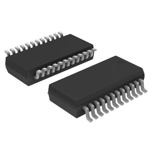
- Package: SSOP (Shrink Small Outline Package)
- Essence: Voltage level shifting between different logic families
- Packaging/Quantity: Tape and Reel, 2500 units per reel
Specifications
- Supply Voltage Range: 2.7V to 3.6V
- Logic Family: LVT (Low Voltage TTL)
- Number of Channels: 8
- Input Voltage Levels: 5V Tolerant
- Output Voltage Levels: 3.3V
- Maximum Data Rate: 400 Mbps
Detailed Pin Configuration
- OE (Output Enable) - Active Low
- A1 - Channel 1 Control Input
- B1 - Channel 1 Control Input
- Y1 - Channel 1 Output
- GND (Ground)
- Y2 - Channel 2 Output
- B2 - Channel 2 Control Input
- A2 - Channel 2 Control Input
- VCC (Supply Voltage)
- GND (Ground)
- A3 - Channel 3 Control Input
- B3 - Channel 3 Control Input
- Y3 - Channel 3 Output
- OE (Output Enable) - Active Low
- Y4 - Channel 4 Output
- B4 - Channel 4 Control Input
- A4 - Channel 4 Control Input
- GND (Ground)
- Y5 - Channel 5 Output
- B5 - Channel 5 Control Input
- A5 - Channel 5 Control Input
- VCC (Supply Voltage)
- GND (Ground)
- A6 - Channel 6 Control Input
- B6 - Channel 6 Control Input
- Y6 - Channel 6 Output
- OE (Output Enable) - Active Low
- Y7 - Channel 7 Output
- B7 - Channel 7 Control Input
- A7 - Channel 7 Control Input
- GND (Ground)
- Y8 - Channel 8 Output
- B8 - Channel 8 Control Input
- A8 - Channel 8 Control Input
- VCC (Supply Voltage)
- GND (Ground)
- DIR (Direction Control) - Active High
- GND (Ground)
- A9 - Channel 9 Control Input
- B9 - Channel 9 Control Input
- Y9 - Channel 9 Output
- OE (Output Enable) - Active Low
- Y10 - Channel 10 Output
- B10 - Channel 10 Control Input
- A10 - Channel 10 Control Input
- GND (Ground)
- Y11 - Channel 11 Output
- B11 - Channel 11 Control Input
- A11 - Channel 11 Control Input
- VCC (Supply Voltage)
- GND (Ground)
- A12 - Channel 12 Control Input
- B12 - Channel 12 Control Input
- Y12 - Channel 12 Output
- OE (Output Enable) - Active Low
- Y13 - Channel 13 Output
- B13 - Channel 13 Control Input
- A13 - Channel 13 Control Input
- GND (Ground)
- Y14 - Channel 14 Output
- B14 - Channel 14 Control Input
- A14 - Channel 14 Control Input
- VCC (Supply Voltage)
- GND (Ground)
- A15 - Channel 15 Control Input
- B15 - Channel 15 Control Input
- Y15 - Channel 15 Output
- OE (Output Enable) - Active Low
- Y16 - Channel 16 Output
- B16 - Channel 16 Control Input
- A16 - Channel 16 Control Input
- GND (Ground)
- Y17 - Channel 17 Output
- B17 - Channel 17 Control Input
- A17 - Channel 17 Control Input
- VCC (Supply Voltage)
- GND (Ground)
- A18 - Channel 18 Control Input
- B18 - Channel 18 Control Input
- Y18 - Channel 18 Output
- OE (Output Enable) - Active Low
- Y19 - Channel 19 Output
- B19 - Channel 19 Control Input
- A19 - Channel 19 Control Input
- GND (
技術ソリューションにおける 74LVT652DB,118 の適用に関連する 10 件の一般的な質問と回答をリストします。
Sure! Here are 10 common questions and answers related to the application of 74LVT652DB,118:
Q: What is the function of the 74LVT652DB,118? A: The 74LVT652DB,118 is an octal transceiver with 3-state outputs. It can be used for bidirectional data transfer between buses operating at different voltage levels.
Q: What is the voltage range supported by the 74LVT652DB,118? A: The 74LVT652DB,118 supports a voltage range of 1.65V to 3.6V.
Q: How many channels does the 74LVT652DB,118 have? A: The 74LVT652DB,118 has 8 bidirectional channels.
Q: Can the 74LVT652DB,118 handle high-speed data transfer? A: Yes, the 74LVT652DB,118 is designed to support high-speed data transfer up to 400Mbps.
Q: Is the 74LVT652DB,118 compatible with TTL logic levels? A: No, the 74LVT652DB,118 operates with CMOS logic levels and is not directly compatible with TTL logic.
Q: Can the 74LVT652DB,118 be used as a level shifter? A: Yes, the 74LVT652DB,118 can be used as a level shifter to interface between different voltage domains.
Q: Does the 74LVT652DB,118 have internal pull-up or pull-down resistors? A: No, the 74LVT652DB,118 does not have internal pull-up or pull-down resistors.
Q: What is the maximum current that can be sourced or sunk by the outputs of 74LVT652DB,118? A: The maximum output current for each channel of the 74LVT652DB,118 is typically ±24mA.
Q: Can the 74LVT652DB,118 be used in hot-swapping applications? A: Yes, the 74LVT652DB,118 supports hot insertion and extraction of modules without causing damage to the device.
Q: Are there any specific precautions to consider when using the 74LVT652DB,118? A: It is important to ensure proper decoupling capacitors are placed near the power supply pins of the 74LVT652DB,118 to minimize noise and voltage fluctuations. Additionally, care should be taken to avoid exceeding the absolute maximum ratings specified in the datasheet.
Please note that these answers are general and may vary depending on the specific requirements and application context. Always refer to the datasheet and consult with the manufacturer for detailed information.