

74LVT543DB,112
Basic Information Overview
- Category: Integrated Circuit (IC)
- Use: Level Shifter and Bus Transceiver
- Characteristics: Low Voltage, Tri-State Outputs, High-Speed Operation
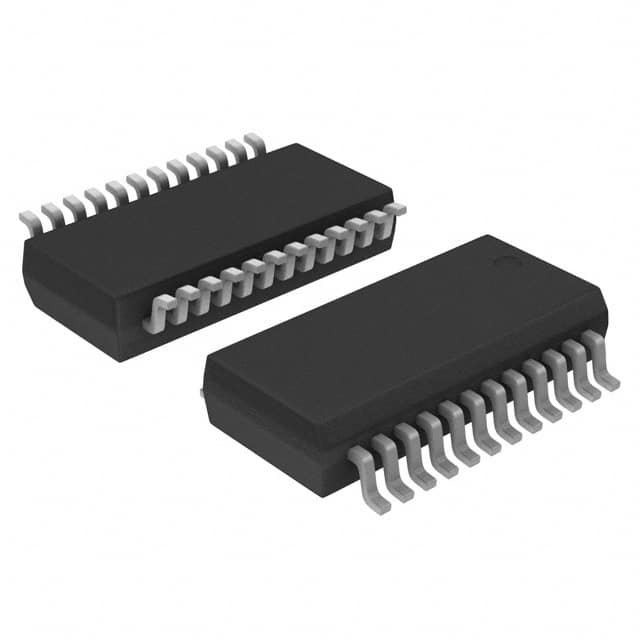
- Package: SSOP-24
- Essence: Logic IC for voltage level translation and bidirectional data transfer between different voltage domains
- Packaging/Quantity: Tape and Reel, 2500 pieces per reel
Specifications
- Supply Voltage Range: 1.2V to 3.6V
- Input Voltage Range: 0V to VCC
- Output Voltage Range: 0V to VCC
- Operating Temperature Range: -40°C to +85°C
- Propagation Delay Time: 4.5ns (Max)
- Output Current: ±12mA
- Input Capacitance: 3pF (Typ)
Detailed Pin Configuration
The 74LVT543DB,112 IC has a total of 24 pins arranged as follows:
+-------------------+
    OE1 --|1                24|-- VCC
   DIR1 --|2                23|-- GND
   A1B1 --|3                22|-- B1A1
   A2B2 --|4                21|-- B2A2
   A3B3 --|5                20|-- B3A3
   A4B4 --|6                19|-- B4A4
   A5B5 --|7                18|-- B5A5
   A6B6 --|8                17|-- B6A6
   A7B7 --|9                16|-- B7A7
   A8B8 --|10               15|-- B8A8
   GND --|11               14|-- OE2
   VCC --|12               13|-- DIR2
          +-------------------+
Functional Features
- Bidirectional voltage level translation between two different voltage domains
- Tri-state outputs allow multiple devices to share a common bus
- High-speed operation for efficient data transfer
- Low voltage operation for power efficiency
Advantages and Disadvantages
Advantages
- Enables communication between devices operating at different voltage levels
- Supports bidirectional data transfer
- Tri-state outputs facilitate bus sharing
- High-speed operation allows for efficient data transmission
Disadvantages
- Limited to specific voltage ranges (1.2V to 3.6V)
- Requires careful consideration of input and output voltage compatibility
Working Principles
The 74LVT543DB,112 is designed to translate logic signals between two voltage domains. It utilizes a combination of level shifting circuitry and tri-state buffers to achieve bidirectional data transfer. The direction of data flow is controlled by the DIR1 and DIR2 pins. When enabled, the IC translates and transfers data from one domain to the other. When disabled, the outputs are in a high-impedance state, allowing other devices to drive the bus.
Detailed Application Field Plans
The 74LVT543DB,112 is commonly used in various applications where voltage level translation and bidirectional data transfer are required. Some typical application fields include: - Communication systems - Data acquisition systems - Industrial automation - Consumer electronics - Automotive electronics
Detailed and Complete Alternative Models
- 74LVC543A: Similar functionality with slightly different specifications
- SN74LVC543A: Equivalent alternative from Texas Instruments
- MC74LVC543: Alternative model from ON Semiconductor
(Note: This list is not exhaustive and there may be other alternative models available in the market.)
This entry provides an overview of the 74LVT543DB,112 integrated circuit. It includes basic information about its category, use, characteristics, package, and essence. The specifications, pin configuration, functional features, advantages and disadvantages, working principles, application field plans, and alternative models are also discussed.
技術ソリューションにおける 74LVT543DB,112 の適用に関連する 10 件の一般的な質問と回答をリストします。
Sure! Here are 10 common questions and answers related to the application of 74LVT543DB,112 in technical solutions:
Q: What is the function of the 74LVT543DB,112? A: The 74LVT543DB,112 is an octal transceiver with tri-state outputs. It can be used for bidirectional data transfer between two buses.
Q: What is the operating voltage range of the 74LVT543DB,112? A: The 74LVT543DB,112 operates within a voltage range of 2.7V to 3.6V.
Q: How many channels does the 74LVT543DB,112 have? A: The 74LVT543DB,112 has 8 channels, allowing for simultaneous bidirectional data transfer on each channel.
Q: Can the 74LVT543DB,112 handle high-speed data transfer? A: Yes, the 74LVT543DB,112 is designed for high-speed operation and can support data rates up to 400Mbps.
Q: Does the 74LVT543DB,112 have built-in protection features? A: Yes, the 74LVT543DB,112 has built-in ESD protection on all inputs and outputs, ensuring robustness against electrostatic discharge.
Q: Can the 74LVT543DB,112 be used in both parallel and serial communication systems? A: Yes, the 74LVT543DB,112 can be used in both parallel and serial communication systems, depending on the application requirements.
Q: What is the maximum output current of the 74LVT543DB,112? A: The 74LVT543DB,112 can provide a maximum output current of 12mA per channel.
Q: Does the 74LVT543DB,112 have internal pull-up or pull-down resistors? A: No, the 74LVT543DB,112 does not have internal pull-up or pull-down resistors. External resistors may be required for proper signal termination.
Q: Can the 74LVT543DB,112 be used in mixed-voltage systems? A: Yes, the 74LVT543DB,112 has voltage translation capabilities, allowing it to interface between different voltage domains.
Q: What is the package type of the 74LVT543DB,112? A: The 74LVT543DB,112 is available in a TSSOP-20 package, which is a surface-mount package with 20 pins.
Please note that the answers provided here are general and may vary depending on specific application requirements. It's always recommended to refer to the datasheet and consult the manufacturer for detailed information.