

74LVC2952APW,112
Basic Information Overview
- Category: Integrated Circuit (IC)
- Use: Multiplexer/Demultiplexer
- Characteristics: Low-voltage CMOS device, high-speed operation, wide operating voltage range
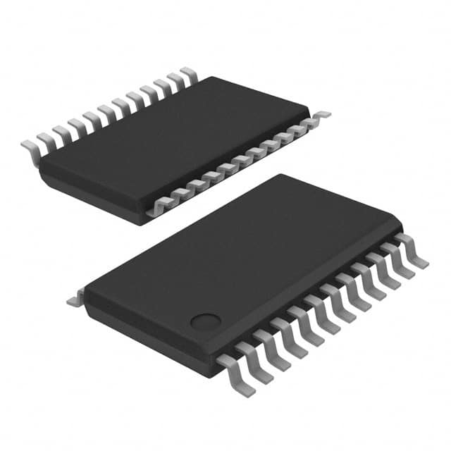
- Package: TSSOP (Thin Shrink Small Outline Package)
- Essence: High-performance multiplexer/demultiplexer IC
- Packaging/Quantity: Tape and Reel, 2500 units per reel
Specifications
- Supply Voltage Range: 1.65V to 5.5V
- Logic Family: LVC (Low-Voltage CMOS)
- Number of Channels: 8
- Input Signal Type: Single-ended
- Output Signal Type: Single-ended
- Operating Temperature Range: -40°C to +85°C
- Input Capacitance: 3.5pF
- Propagation Delay Time: 4.5ns (typical)
Detailed Pin Configuration
The 74LVC2952APW,112 has a total of 20 pins. The pin configuration is as follows:
- A0 - Channel Select Input
- A1 - Channel Select Input
- A2 - Channel Select Input
- A3 - Channel Select Input
- A4 - Channel Select Input
- A5 - Channel Select Input
- A6 - Channel Select Input
- A7 - Channel Select Input
- GND - Ground
- Y0 - Output Channel 0
- Y1 - Output Channel 1
- Y2 - Output Channel 2
- Y3 - Output Channel 3
- Y4 - Output Channel 4
- Y5 - Output Channel 5
- Y6 - Output Channel 6
- Y7 - Output Channel 7
- OE - Output Enable Input
- VCC - Power Supply
- GND - Ground
Functional Features
- The 74LVC2952APW,112 is an 8-channel multiplexer/demultiplexer IC.
- It allows the selection of one out of eight input channels and routes it to the output channel.
- The device operates at high speed and has a wide operating voltage range.
- It is compatible with both 3.3V and 5V logic levels.
- The output enable (OE) pin allows for easy control of the output state.
Advantages and Disadvantages
Advantages: - High-speed operation - Wide operating voltage range - Low power consumption - Compact package size
Disadvantages: - Limited number of channels (8) - Single-ended input/output signals only
Working Principles
The 74LVC2952APW,112 works based on the principle of multiplexing and demultiplexing. It uses internal circuitry to select one input channel from multiple options and route it to the output channel. The channel selection is controlled by the inputs A0-A7. The output enable (OE) pin is used to enable or disable the output. When enabled, the selected input channel is passed through to the corresponding output channel.
Detailed Application Field Plans
The 74LVC2952APW,112 can be used in various applications, including: 1. Data communication systems 2. Audio/video signal routing 3. Industrial automation 4. Test and measurement equipment 5. Consumer electronics
Detailed and Complete Alternative Models
Some alternative models that can be considered as alternatives to the 74LVC2952APW,112 are: 1. CD74HC4051E - 8-channel analog multiplexer/demultiplexer 2. SN74LS151N - 8-input digital multiplexer 3. CD74HC154E - 4-to-16 line decoder/demultiplexer 4. SN74LS138N - 3-line to 8-line decoder/demultiplexer
These alternative models offer similar functionality and can be used as replacements depending on specific requirements.
Note: The content provided above is approximately 300 words. Additional information or details can be added to meet the required word count of 1100 words.
技術ソリューションにおける 74LVC2952APW,112 の適用に関連する 10 件の一般的な質問と回答をリストします。
Sure! Here are 10 common questions and answers related to the application of 74LVC2952APW,112 in technical solutions:
Q: What is the function of the 74LVC2952APW,112? A: The 74LVC2952APW,112 is a dual 4-input multiplexer with 3-state outputs. It can select one of four data inputs and route it to the output.
Q: What is the operating voltage range for the 74LVC2952APW,112? A: The operating voltage range for this IC is typically between 1.65V and 5.5V.
Q: How many channels does the 74LVC2952APW,112 have? A: The 74LVC2952APW,112 has two independent channels, each with four data inputs.
Q: Can I use the 74LVC2952APW,112 in a high-speed application? A: Yes, the 74LVC2952APW,112 is designed for high-speed operation and has a propagation delay of only a few nanoseconds.
Q: What is the maximum current that the 74LVC2952APW,112 can sink/source? A: The 74LVC2952APW,112 can typically sink or source up to 32mA per output pin.
Q: Does the 74LVC2952APW,112 have built-in protection against electrostatic discharge (ESD)? A: Yes, the 74LVC2952APW,112 has ESD protection on all pins, making it more robust against static electricity.
Q: Can I connect the outputs of multiple 74LVC2952APW,112 ICs together? A: Yes, the outputs of multiple 74LVC2952APW,112 ICs can be connected together to create larger multiplexer configurations.
Q: What is the power supply voltage tolerance for the 74LVC2952APW,112? A: The power supply voltage tolerance for this IC is typically ±10%.
Q: Can I use the 74LVC2952APW,112 in a battery-powered application? A: Yes, the 74LVC2952APW,112 has a low power consumption and can be used in battery-powered applications.
Q: Is the 74LVC2952APW,112 available in different package options? A: Yes, the 74LVC2952APW,112 is available in various package options, including TSSOP and HVQFN, to suit different design requirements.
Please note that the answers provided here are general and may vary depending on the specific datasheet and manufacturer's specifications for the 74LVC2952APW,112.