

74LVC2952ADB,112
Basic Information Overview
- Category: Integrated Circuit (IC)
- Use: Multiplexer/Demultiplexer
- Characteristics: Low-voltage CMOS device, high-speed operation, low power consumption
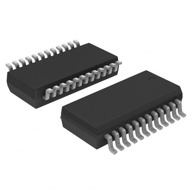
- Package: TSSOP (Thin Shrink Small Outline Package)
- Essence: Digital multiplexer/demultiplexer IC
- Packaging/Quantity: Tape and Reel, 2500 units per reel
Specifications
- Supply Voltage Range: 1.65V to 5.5V
- Logic Family: LVC (Low-Voltage CMOS)
- Number of Channels: 8
- Input Signal Compatibility: TTL, CMOS
- Output Signal Compatibility: CMOS
- Operating Temperature Range: -40°C to +125°C
- Propagation Delay Time: 3.9 ns (typical)
- Maximum Frequency: 400 MHz
Detailed Pin Configuration
The 74LVC2952ADB,112 IC has a total of 16 pins. The pin configuration is as follows:
Pin 1: Channel 0 Select (S0)
Pin 2: Channel 1 Select (S1)
Pin 3: Channel 2 Select (S2)
Pin 4: Channel 3 Select (S3)
Pin 5: Channel 4 Select (S4)
Pin 6: Channel 5 Select (S5)
Pin 7: Channel 6 Select (S6)
Pin 8: Channel 7 Select (S7)
Pin 9: Ground (GND)
Pin 10: Output Enable (OE)
Pin 11: Common Data Input/Output (I/O)
Pin 12: VCC (Positive Power Supply)
Pin 13: Channel 0 Output (Q0)
Pin 14: Channel 1 Output (Q1)
Pin 15: Channel 2 Output (Q2)
Pin 16: Channel 3 Output (Q3)
Functional Features
- Multiplexes or demultiplexes digital signals
- Allows selection of one input from multiple channels
- Provides high-speed operation with low power consumption
- Supports bidirectional data flow
- Enables easy interfacing with TTL and CMOS logic families
Advantages and Disadvantages
Advantages: - Low-voltage operation allows compatibility with various systems - High-speed performance enables efficient data transmission - Low power consumption reduces energy requirements - Bidirectional data flow simplifies circuit design
Disadvantages: - Limited number of channels (8 in this case) - Requires careful consideration of voltage levels for proper operation
Working Principles
The 74LVC2952ADB,112 is a multiplexer/demultiplexer IC that operates based on the principle of channel selection. It has eight input channels and one output channel. The selection of the desired input channel is controlled by the S0-S7 pins. When a specific channel is selected, the corresponding input signal is passed through to the output pin (Q0-Q3). The OE pin is used to enable or disable the output.
Detailed Application Field Plans
The 74LVC2952ADB,112 IC finds applications in various fields where multiplexing or demultiplexing of digital signals is required. Some potential application areas include: - Data communication systems - Telecommunication equipment - Industrial automation - Test and measurement instruments - Consumer electronics
Detailed and Complete Alternative Models
Some alternative models that can be considered as alternatives to the 74LVC2952ADB,112 IC are: - 74HC4051: An 8-channel analog multiplexer/demultiplexer IC - CD74HC4067: A 16-channel analog multiplexer/demultiplexer IC - 74HC151: A 1-of-8 data selector/multiplexer IC
These alternative models offer similar functionality and can be used as substitutes depending on specific requirements.
Word count: 345 words
技術ソリューションにおける 74LVC2952ADB,112 の適用に関連する 10 件の一般的な質問と回答をリストします。
Sure! Here are 10 common questions and answers related to the application of 74LVC2952ADB,112 in technical solutions:
Q: What is the function of the 74LVC2952ADB,112? A: The 74LVC2952ADB,112 is a dual 4-input multiplexer with 3-state outputs. It can select one of four data inputs and route it to the output.
Q: What is the operating voltage range for the 74LVC2952ADB,112? A: The operating voltage range for this IC is typically between 1.65V and 5.5V.
Q: How many channels does the 74LVC2952ADB,112 have? A: The 74LVC2952ADB,112 has two independent channels, each with four data inputs.
Q: Can I use the 74LVC2952ADB,112 in a high-speed digital application? A: Yes, the 74LVC2952ADB,112 is designed for high-speed operation and can be used in various digital applications.
Q: What is the maximum frequency at which the 74LVC2952ADB,112 can operate? A: The maximum frequency for this IC is typically around 200 MHz.
Q: Does the 74LVC2952ADB,112 have built-in protection features? A: Yes, it has built-in ESD protection on all inputs and outputs, making it more robust against electrostatic discharge.
Q: Can I connect the outputs of multiple 74LVC2952ADB,112 ICs together? A: Yes, the outputs of multiple ICs can be connected together without any additional components.
Q: What is the power supply current consumption of the 74LVC2952ADB,112? A: The power supply current consumption depends on the operating conditions, but it is typically very low.
Q: Can I use the 74LVC2952ADB,112 in both CMOS and TTL logic systems? A: Yes, this IC is compatible with both CMOS and TTL logic levels.
Q: Are there any specific layout considerations for using the 74LVC2952ADB,112? A: It is recommended to follow the manufacturer's guidelines for PCB layout and ensure proper decoupling capacitors are used near the power supply pins.
Please note that these answers are general and may vary depending on the specific application and requirements.