

Encyclopedia Entry: 74LVC594ABQ-Q100X
Product Overview
Category
The 74LVC594ABQ-Q100X belongs to the category of integrated circuits (ICs) and specifically falls under the family of shift registers.
Use
This IC is primarily used for serial-in, parallel-out data shifting in various digital applications. It enables efficient data transfer and control in electronic systems.
Characteristics
- Low-voltage CMOS technology
- High-speed operation
- Wide operating voltage range
- Schmitt-trigger action on all inputs
- Output capability: 4 mA at 3.3 V
- Power-down mode
- Overvoltage-tolerant inputs
- ESD protection: HBM JESD22-A114E exceeds 2000 V; MM JESD22-A115-A exceeds 200 V
Package
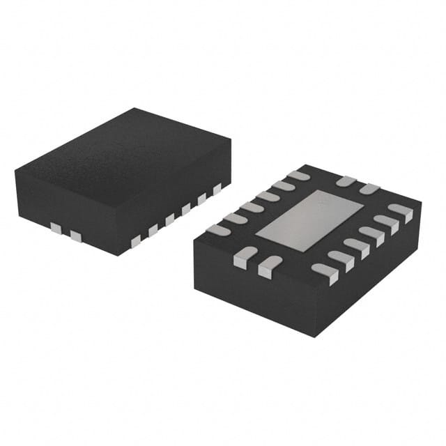
The 74LVC594ABQ-Q100X is available in a compact and industry-standard SSOP (Shrink Small Outline Package) with 16 pins. This package ensures easy integration into circuit boards and provides mechanical stability.
Essence
The essence of the 74LVC594ABQ-Q100X lies in its ability to efficiently shift and control data in digital systems, enabling seamless communication between different components.
Packaging/Quantity
This IC is typically packaged in reels or tubes, with each reel containing 2500 units or each tube containing 90 units.
Specifications
- Supply voltage range: 1.2 V to 3.6 V
- Input voltage range: -0.5 V to +7 V
- Operating temperature range: -40°C to +125°C
- Maximum clock frequency: 100 MHz
- Number of output pins: 8
- Serial data input: Single-ended, non-inverting
Detailed Pin Configuration
The 74LVC594ABQ-Q100X has 16 pins, each serving a specific purpose. The pin configuration is as follows:
- Q0: Output pin 0
- Q1: Output pin 1
- Q2: Output pin 2
- Q3: Output pin 3
- Q4: Output pin 4
- Q5: Output pin 5
- Q6: Output pin 6
- Q7: Output pin 7
- GND: Ground
- SER: Serial data input
- SRCLK: Shift register clock input
- RCLK: Register clock input
- OE: Output enable input
- VCC: Supply voltage
- QAUX: Auxiliary output
- SOUT: Serial data output
Functional Features
- Serial-in, parallel-out shifting of data
- High-speed operation for efficient data transfer
- Schmitt-trigger action on all inputs for noise immunity
- Power-down mode for reduced power consumption
- Overvoltage-tolerant inputs for enhanced robustness
- ESD protection exceeding industry standards
Advantages and Disadvantages
Advantages
- Low-voltage CMOS technology ensures compatibility with modern digital systems.
- Wide operating voltage range allows flexibility in various applications.
- High-speed operation enables rapid data transfer.
- Schmitt-trigger action on inputs enhances noise immunity.
- Power-down mode reduces power consumption when not in use.
- Overvoltage-tolerant inputs provide protection against voltage spikes.
- ESD protection exceeds industry standards, ensuring reliability.
Disadvantages
- Limited number of output pins (8) may restrict certain applications requiring more outputs.
- Requires careful handling to prevent damage due to electrostatic discharge.
Working Principles
The 74LVC594ABQ-Q100X operates based on the principle of serial-in, parallel-out shifting. It receives data serially through the SER pin and shifts it into its internal register upon receiving a clock signal (SRCLK). The register clock input (RCLK) then latches the shifted data into the output pins (Q0-Q7). The output enable input (OE) controls the activation of the outputs.
Detailed Application Field Plans
The 74LVC594ABQ-Q100X finds applications in various digital systems, including but not limited to: - Data communication equipment - Industrial automation - Consumer electronics - Automotive electronics - Medical devices - Robotics
Detailed and Complete Alternative Models
- 74HC595: Similar shift register IC with 8-bit parallel-out capability.
- SN74LS164: Shift register IC with serial-in, parallel-out functionality.
- CD4015BE: Dual 4-stage static shift register IC.
These alternative models offer similar functionalities and can be used as substitutes for the 74LVC594ABQ-Q100X depending on specific requirements.
In conclusion, the 74LVC594ABQ-Q100X is a versatile
技術ソリューションにおける 74LVC594ABQ-Q100X の適用に関連する 10 件の一般的な質問と回答をリストします。
Sure! Here are 10 common questions and answers related to the application of 74LVC594ABQ-Q100X in technical solutions:
Question: What is the purpose of the 74LVC594ABQ-Q100X?
- Answer: The 74LVC594ABQ-Q100X is an 8-bit shift register with output latches, used for serial-to-parallel data conversion.Question: What is the operating voltage range of the 74LVC594ABQ-Q100X?
- Answer: The operating voltage range is from 1.65V to 5.5V.Question: How many outputs does the 74LVC594ABQ-Q100X have?
- Answer: It has 8 outputs that can be individually controlled.Question: Can the 74LVC594ABQ-Q100X be cascaded to control more than 8 outputs?
- Answer: Yes, multiple 74LVC594ABQ-Q100X chips can be cascaded together to control a larger number of outputs.Question: What is the maximum data transfer rate supported by the 74LVC594ABQ-Q100X?
- Answer: The maximum data transfer rate is 100 MHz.Question: Does the 74LVC594ABQ-Q100X have built-in protection features?
- Answer: Yes, it has built-in ESD protection on all inputs and outputs.Question: Can the 74LVC594ABQ-Q100X be used in automotive applications?
- Answer: Yes, the 74LVC594ABQ-Q100X is qualified for automotive applications and meets the AEC-Q100 standard.Question: What is the power supply current consumption of the 74LVC594ABQ-Q100X?
- Answer: The power supply current consumption is typically 2.5 mA.Question: Can the 74LVC594ABQ-Q100X be used in both parallel and serial data transfer modes?
- Answer: Yes, it supports both parallel and serial data transfer modes.Question: What package options are available for the 74LVC594ABQ-Q100X?
- Answer: The 74LVC594ABQ-Q100X is available in a small outline package (SO) and a thin shrink small outline package (TSSOP).
Please note that these answers are general and may vary depending on the specific datasheet and application requirements.