

74LVC1G99GS,115
Basic Information Overview
- Category: Integrated Circuit (IC)
- Use: Logic Gate
- Characteristics: Single Buffer/Driver, Non-Inverting, Schmitt Trigger
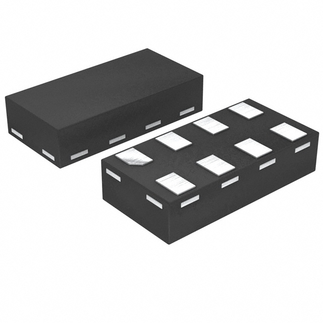
- Package: SOT753 (SC-70)
- Essence: High-Speed CMOS Technology
- Packaging/Quantity: Tape and Reel, 3000 pieces per reel
Specifications
- Supply Voltage Range: 1.65V to 5.5V
- Input Voltage Range: -0.5V to VCC + 0.5V
- Output Voltage Range: GND to VCC
- Maximum Operating Frequency: 400 MHz
- Propagation Delay: 3.8 ns (typical)
- Input Capacitance: 2 pF (typical)
- Output Current: ±24 mA
Detailed Pin Configuration
The 74LVC1G99GS,115 IC has the following pin configuration:
____
   A |1    6| VCC
   B |2    5| Y
 GND |3    4| OE
      ------
Functional Features
- Single buffer/driver with non-inverting output
- Schmitt trigger input for noise immunity
- Wide supply voltage range allows compatibility with various systems
- High-speed operation suitable for time-critical applications
- Low power consumption
- ESD protection for robustness
Advantages and Disadvantages
Advantages: - Small package size enables space-saving designs - Wide supply voltage range enhances versatility - Schmitt trigger input ensures reliable operation in noisy environments - High-speed performance meets demanding requirements
Disadvantages: - Limited output current may not be suitable for driving heavy loads - Single buffer/driver functionality restricts certain applications requiring multiple outputs
Working Principles
The 74LVC1G99GS,115 is a single buffer/driver IC that takes an input signal and provides a non-inverted output. It incorporates a Schmitt trigger input, which helps in reducing the effects of noise and ensuring stable operation even in noisy environments. The IC operates within a wide supply voltage range, making it compatible with various systems. It utilizes high-speed CMOS technology, allowing for fast switching times and efficient performance.
Detailed Application Field Plans
The 74LVC1G99GS,115 finds applications in various fields, including but not limited to: - Communication systems - Industrial automation - Consumer electronics - Automotive electronics - Medical devices
In communication systems, this IC can be used for signal conditioning, level shifting, and interfacing between different logic families. In industrial automation, it can be employed for sensor interfacing, motor control, and general-purpose digital logic functions. In consumer electronics, it can be utilized for audio/video signal processing, data transmission, and control circuitry. In automotive electronics, it can find applications in engine control units, lighting systems, and dashboard displays. In medical devices, it can be used for patient monitoring, diagnostic equipment, and data acquisition.
Detailed and Complete Alternative Models
Some alternative models to the 74LVC1G99GS,115 IC include: - SN74LVC1G99DBVR (Texas Instruments) - MC74LVC1G99 (ON Semiconductor) - NCV8180 (ON Semiconductor) - TC7SZU04FU (Toshiba) - 74AUP1G99GW (NXP Semiconductors)
These alternatives offer similar functionality and characteristics, providing options for designers based on specific requirements and availability.
Word count: 343 words
技術ソリューションにおける 74LVC1G99GS,115 の適用に関連する 10 件の一般的な質問と回答をリストします。
Sure! Here are 10 common questions and answers related to the application of 74LVC1G99GS,115 in technical solutions:
Q1: What is the function of the 74LVC1G99GS,115? A1: The 74LVC1G99GS,115 is a single 8-input multiplexer/demultiplexer with three-state outputs. It can be used to select one of eight input signals and route it to the output.
Q2: What is the operating voltage range for the 74LVC1G99GS,115? A2: The operating voltage range for the 74LVC1G99GS,115 is from 1.65V to 5.5V.
Q3: How many inputs does the 74LVC1G99GS,115 have? A3: The 74LVC1G99GS,115 has 8 inputs.
Q4: Can the 74LVC1G99GS,115 be used as a demultiplexer? A4: Yes, the 74LVC1G99GS,115 can be used as both a multiplexer and a demultiplexer.
Q5: What is the maximum output current of the 74LVC1G99GS,115? A5: The maximum output current of the 74LVC1G99GS,115 is 32mA.
Q6: Does the 74LVC1G99GS,115 have three-state outputs? A6: Yes, the 74LVC1G99GS,115 has three-state outputs, which means that the outputs can be disabled and put into a high-impedance state.
Q7: Can the 74LVC1G99GS,115 be cascaded to increase the number of inputs? A7: Yes, multiple 74LVC1G99GS,115 can be cascaded together to increase the number of inputs.
Q8: What is the propagation delay of the 74LVC1G99GS,115? A8: The propagation delay of the 74LVC1G99GS,115 is typically around 4.5ns.
Q9: Is the 74LVC1G99GS,115 compatible with other logic families? A9: Yes, the 74LVC1G99GS,115 is compatible with both CMOS and TTL logic families.
Q10: Can the 74LVC1G99GS,115 be used in battery-powered applications? A10: Yes, the 74LVC1G99GS,115 is suitable for battery-powered applications due to its low power consumption.
Please note that these answers are general and may vary depending on specific application requirements.