

74LVC162245ADL,112
Basic Information Overview
- Category: Integrated Circuit (IC)
- Use: Level Shifter and Buffer
- Characteristics: Bi-directional voltage level translation between different logic levels
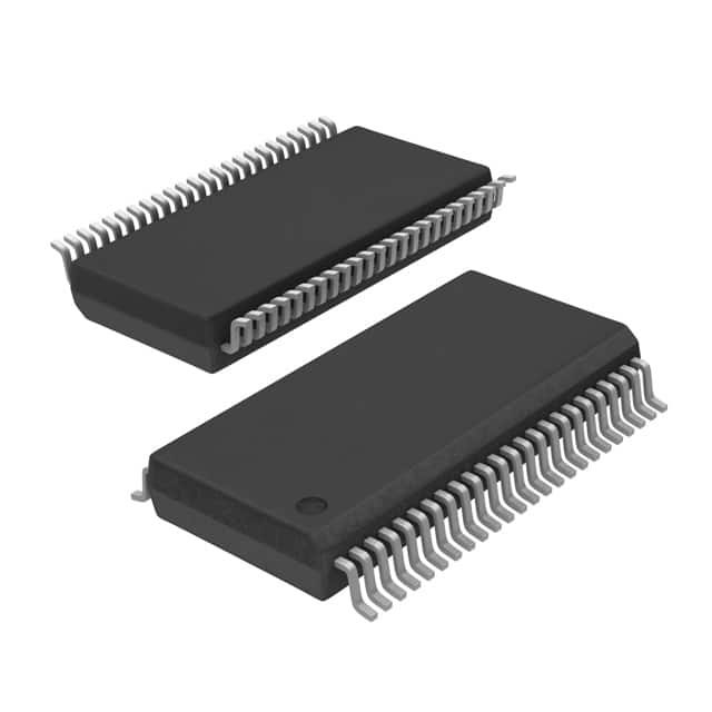
- Package: TSSOP (Thin Shrink Small Outline Package)
- Essence: High-speed CMOS technology for low power consumption and high noise immunity
- Packaging/Quantity: Tape and Reel, 2500 units per reel
Specifications
- Number of Channels: 16
- Logic Family: LVC (Low Voltage CMOS)
- Supply Voltage Range: 1.2V to 3.6V
- Input Voltage Range: GND to VCC
- Output Voltage Range: GND to VCC
- Maximum Operating Frequency: 400 MHz
- Propagation Delay: 4.5 ns (max) at 3.3V supply
- Output Drive Capability: ±24 mA
- ESD Protection: Human Body Model >2000V, Machine Model >200V
Detailed Pin Configuration
The 74LVC162245ADL,112 IC has a total of 48 pins arranged in a TSSOP package. The pin configuration is as follows:
+-------------------+
   OE1 |1                 48| VCC
   A1  |2                 47| B1
   A2  |3                 46| B2
   A3  |4                 45| B3
   A4  |5                 44| B4
   A5  |6                 43| B5
   A6  |7                 42| B6
   A7  |8                 41| B7
   A8  |9                 40| B8
   A9  |10                39| B9
   A10 |11                38| B10
   A11 |12                37| B11
   A12 |13                36| B12
   A13 |14                35| B13
   A14 |15                34| B14
   A15 |16                33| B15
   GND |17                32| VCC
   DIR |18                31| OE2
   BDIR|19                30| A16
   B16 |20                29| A15
   B15 |21                28| A14
   B14 |22                27| A13
   B13 |23                26| A12
   B12 |24                25| A11
        +-------------------+
Functional Features
- Bi-directional voltage level translation: Allows for seamless communication between devices operating at different logic levels.
- High-speed operation: Supports data rates up to 400 MHz, making it suitable for high-performance applications.
- Low power consumption: Utilizes CMOS technology to minimize power consumption and extend battery life in portable devices.
- High noise immunity: Provides robust performance in noisy environments, ensuring reliable data transmission.
Advantages and Disadvantages
Advantages: - Wide supply voltage range allows compatibility with various systems. - Fast propagation delay enables efficient data transfer. - Compact TSSOP package saves board space. - High noise immunity ensures reliable operation.
Disadvantages: - Limited number of channels may not be sufficient for complex applications requiring more I/O lines. - Requires careful consideration of voltage compatibility to prevent damage to connected devices.
Working Principles
The 74LVC162245ADL,112 is a bidirectional level shifter and buffer IC. It translates signals between two different logic voltage levels, allowing devices operating at different voltages to communicate with each other. The direction of data flow is controlled by the DIR and BDIR pins. When DIR is high, data flows from the A-side to the B-side, and when BDIR is high, data flows from the B-side to the A-side.
The IC utilizes high-speed CMOS technology, which provides low power consumption and high noise immunity. It operates within a wide supply voltage range, making it compatible with various systems. The outputs have a high drive capability, enabling them to drive capacitive loads and long traces without signal degradation.
Detailed Application Field Plans
The 74LVC162245ADL,112 is commonly used in various applications that require voltage level translation between different logic levels. Some typical application fields include: - Communication interfaces: UART, SPI, I2C, etc. - Memory interfaces: DDR, SRAM, Flash, etc. - Microcontroller interfacing: Connecting microcontrollers operating at different voltage levels. - Mixed-voltage systems: Bridging the gap between different voltage domains in complex systems.
Detailed and Complete Alternative Models
Some alternative models that
技術ソリューションにおける 74LVC162245ADL,112 の適用に関連する 10 件の一般的な質問と回答をリストします。
Sure! Here are 10 common questions and answers related to the application of 74LVC162245ADL,112 in technical solutions:
Q: What is the function of the 74LVC162245ADL,112? A: The 74LVC162245ADL,112 is a 16-bit bus transceiver with 3-state outputs. It can be used to enable bidirectional communication between two buses.
Q: What is the voltage range supported by the 74LVC162245ADL,112? A: The 74LVC162245ADL,112 supports a voltage range of 1.65V to 5.5V.
Q: How many channels does the 74LVC162245ADL,112 have? A: The 74LVC162245ADL,112 has 16 channels, allowing it to handle 16 bits of data.
Q: Can the 74LVC162245ADL,112 be used for level shifting? A: Yes, the 74LVC162245ADL,112 can be used for level shifting as it supports different voltage levels on its input and output sides.
Q: What is the maximum data transfer rate supported by the 74LVC162245ADL,112? A: The 74LVC162245ADL,112 supports a maximum data transfer rate of 400 Mbps.
Q: Does the 74LVC162245ADL,112 have built-in ESD protection? A: Yes, the 74LVC162245ADL,112 has built-in ESD protection, making it more robust against electrostatic discharge.
Q: Can the 74LVC162245ADL,112 be used in both parallel and serial communication systems? A: Yes, the 74LVC162245ADL,112 can be used in both parallel and serial communication systems, depending on the application requirements.
Q: What is the power supply voltage required for the 74LVC162245ADL,112? A: The 74LVC162245ADL,112 requires a power supply voltage of 1.65V to 5.5V.
Q: Does the 74LVC162245ADL,112 support hot insertion? A: Yes, the 74LVC162245ADL,112 supports hot insertion, allowing it to be inserted or removed from a live circuit without causing damage.
Q: Can the 74LVC162245ADL,112 be cascaded to handle more than 16 bits of data? A: Yes, multiple 74LVC162245ADL,112 devices can be cascaded together to handle more than 16 bits of data by connecting their input and output pins accordingly.
Please note that the specific details and answers may vary based on the datasheet and application requirements.