

Encyclopedia Entry: 74HCT4017BQ-Q100X
Product Overview
Category
The 74HCT4017BQ-Q100X belongs to the category of integrated circuits (ICs) and specifically falls under the family of digital counter ICs.
Use
This product is commonly used in electronic circuits for counting and sequencing applications. It provides a convenient solution for controlling the sequence of events or signals in various electronic systems.
Characteristics
- High-speed operation
- Low power consumption
- Wide operating voltage range
- Schmitt-trigger action on all inputs
- Direct interface with TTL levels
- Buffered outputs for cascading
- Compact and durable package design
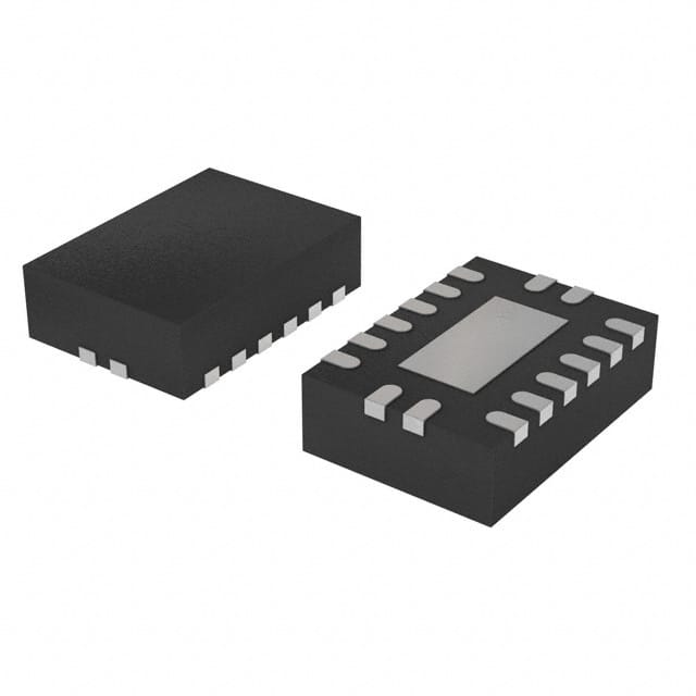
Package
The 74HCT4017BQ-Q100X is available in a small outline, surface-mount package (SOIC). This package offers excellent thermal performance and ease of integration into circuit boards.
Essence
The essence of the 74HCT4017BQ-Q100X lies in its ability to provide reliable and efficient counting and sequencing functionality in electronic systems. It simplifies the implementation of sequential logic and enables precise control over the order of events.
Packaging/Quantity
The 74HCT4017BQ-Q100X is typically packaged in reels or tubes, containing a specified quantity of ICs per package. The exact packaging and quantity may vary depending on the manufacturer and supplier.
Specifications
- Supply Voltage Range: 2V to 6V
- Operating Temperature Range: -40°C to +125°C
- Maximum Clock Frequency: 25 MHz
- Number of Outputs: 10
- Logic Family: HCT
- Input Type: Schmitt Trigger
- Output Type: Buffered
Detailed Pin Configuration
The 74HCT4017BQ-Q100X has a total of 16 pins, each serving a specific function. The pin configuration is as follows:
- Clock (CLK)
- Enable (EN)
- Reset (RST)
- Output 5 (Q5)
- Output 1 (Q1)
- Output 0 (Q0)
- Output 2 (Q2)
- Output 6 (Q6)
- Output 7 (Q7)
- Output 3 (Q3)
- Output 8 (Q8)
- Output 9 (Q9)
- Output 4 (Q4)
- Carry Out (CO)
- Ground (GND)
- Supply Voltage (VCC)
Functional Features
The 74HCT4017BQ-Q100X offers the following functional features:
- Decade counter with 10 decoded outputs
- Direct reset and enable inputs for easy control
- Cascadable for larger counting applications
- Schmitt-trigger inputs for noise immunity
- Buffered outputs for driving external circuitry
Advantages and Disadvantages
Advantages
- High-speed operation allows for efficient counting and sequencing.
- Low power consumption makes it suitable for battery-powered devices.
- Wide operating voltage range provides flexibility in various applications.
- Schmitt-trigger action on all inputs ensures reliable performance in noisy environments.
- Direct interface with TTL levels simplifies integration with existing systems.
- Buffered outputs enable cascading of multiple counters.
Disadvantages
- Limited number of outputs may restrict certain complex applications.
- Lack of built-in error detection or correction mechanisms.
Working Principles
The 74HCT4017BQ-Q100X operates based on the principles of digital counting and sequential logic. It utilizes internal flip-flops to store and propagate binary values, allowing for accurate counting from one state to another. The clock input triggers the transition between states, while the enable and reset inputs provide control over the counting sequence.
Detailed Application Field Plans
The 74HCT4017BQ-Q100X finds applications in various fields, including:
- Electronic instrumentation: Used for event sequencing and timing control in test and measurement equipment.
- Lighting control systems: Enables sequential switching of lights or LEDs in decorative lighting setups.
- Audio equipment: Provides precise control over audio effects and signal routing in mixers and synthesizers.
- Industrial automation: Utilized for controlling the sequence of operations in manufacturing processes.
- Automotive electronics: Integrated into vehicle systems for functions like turn signal sequencing and dashboard displays.
Detailed and Complete Alternative Models
There are several alternative models available that offer similar functionality to the 74HCT4017BQ-Q100X. Some notable alternatives include:
- CD4017
- MC14017
- HEF4017
- SN74HC4017
These alternatives may differ in terms of specific characteristics, pin configuration, or package type, but they serve the same purpose of digital counting and sequencing.
In conclusion, the 74HCT4017BQ-Q100X is a
技術ソリューションにおける 74HCT4017BQ-Q100X の適用に関連する 10 件の一般的な質問と回答をリストします。
Sure! Here are 10 common questions and answers related to the application of 74HCT4017BQ-Q100X in technical solutions:
Question: What is the purpose of the 74HCT4017BQ-Q100X?
Answer: The 74HCT4017BQ-Q100X is a high-speed CMOS counter/divider IC that can be used for various applications such as frequency division, sequencing, and control signal generation.Question: What is the maximum clock frequency supported by the 74HCT4017BQ-Q100X?
Answer: The 74HCT4017BQ-Q100X can operate at a maximum clock frequency of 25 MHz.Question: How many outputs does the 74HCT4017BQ-Q100X have?
Answer: The 74HCT4017BQ-Q100X has 10 outputs, labeled Q0 to Q9.Question: Can the 74HCT4017BQ-Q100X be cascaded to increase the number of outputs?
Answer: Yes, multiple 74HCT4017BQ-Q100X ICs can be cascaded together to increase the number of outputs.Question: What is the power supply voltage range for the 74HCT4017BQ-Q100X?
Answer: The 74HCT4017BQ-Q100X operates with a power supply voltage range of 2 V to 6 V.Question: Does the 74HCT4017BQ-Q100X have any built-in debounce circuitry?
Answer: No, the 74HCT4017BQ-Q100X does not have any built-in debounce circuitry. External debouncing may be required depending on the application.Question: Can the 74HCT4017BQ-Q100X be used for frequency division?
Answer: Yes, the 74HCT4017BQ-Q100X can be used as a frequency divider by connecting the clock input to a higher frequency signal and using the appropriate output.Question: What is the maximum output current of the 74HCT4017BQ-Q100X?
Answer: The maximum output current per output pin of the 74HCT4017BQ-Q100X is 4 mA.Question: Is the 74HCT4017BQ-Q100X compatible with both TTL and CMOS logic levels?
Answer: Yes, the 74HCT4017BQ-Q100X is compatible with both TTL and CMOS logic levels, making it versatile for various applications.Question: Can the 74HCT4017BQ-Q100X be used in automotive applications?
Answer: Yes, the 74HCT4017BQ-Q100X is qualified for automotive applications and meets the AEC-Q100 standard.
Please note that these answers are general and may vary depending on the specific datasheet and application requirements.