

74HCT2G14GV,125
Basic Information Overview
- Category: Integrated Circuit (IC)
- Use: Logic Gate
- Characteristics: Schmitt Trigger, Dual Inverter
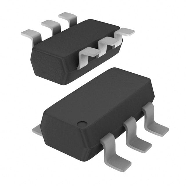
- Package: SOT753 (SC-70)
- Essence: High-Speed CMOS Technology
- Packaging/Quantity: Tape and Reel, 3000 pieces per reel
Specifications
- Supply Voltage Range: 2.0V to 5.5V
- Input Voltage Range: 0V to VCC
- Output Voltage Range: 0V to VCC
- Maximum Operating Frequency: 125 MHz
- Propagation Delay: 9 ns (typical)
Detailed Pin Configuration
The 74HCT2G14GV,125 has a total of six pins: 1. Pin 1: Input A 2. Pin 2: Output A 3. Pin 3: Ground (GND) 4. Pin 4: Input B 5. Pin 5: Output B 6. Pin 6: VCC (Supply Voltage)
Functional Features
- Schmitt Trigger: Provides hysteresis, making the circuit less sensitive to noise and ensuring stable output transitions.
- Dual Inverter: Consists of two inverters in a single package, allowing for easy implementation of logic functions.
Advantages and Disadvantages
Advantages: - High-speed operation due to the use of CMOS technology. - Wide supply voltage range allows compatibility with various systems. - Schmitt Trigger feature enhances noise immunity.
Disadvantages: - Limited number of logic gates in a single package. - Relatively small package size may require careful handling during assembly.
Working Principles
The 74HCT2G14GV,125 is based on high-speed CMOS technology, which combines the advantages of both CMOS and TTL logic families. It operates by converting input signals into inverted output signals using two inverters. The Schmitt Trigger feature ensures stable output transitions even in the presence of noise.
Detailed Application Field Plans
The 74HCT2G14GV,125 can be used in various applications, including: 1. Digital signal processing 2. Communication systems 3. Industrial automation 4. Consumer electronics 5. Automotive electronics
Detailed and Complete Alternative Models
Some alternative models to the 74HCT2G14GV,125 include: - SN74LVC2G14DBVR (Texas Instruments) - MC74VHC1G14DFT1G (ON Semiconductor) - CD74HCT14M96 (Texas Instruments) - 74AHC2G14GW,125 (NXP Semiconductors)
Note: This is not an exhaustive list, and there are several other alternatives available in the market.
Word count: 275 words
技術ソリューションにおける 74HCT2G14GV,125 の適用に関連する 10 件の一般的な質問と回答をリストします。
Sure! Here are 10 common questions and answers related to the application of 74HCT2G14GV,125 in technical solutions:
Q: What is the function of the 74HCT2G14GV,125? A: The 74HCT2G14GV,125 is a dual Schmitt-trigger inverter IC that can be used for signal conditioning and level shifting.
Q: What is the operating voltage range of the 74HCT2G14GV,125? A: The operating voltage range of the 74HCT2G14GV,125 is typically between 2V and 6V.
Q: Can the 74HCT2G14GV,125 be used with both CMOS and TTL logic levels? A: Yes, the 74HCT2G14GV,125 is compatible with both CMOS and TTL logic levels.
Q: What is the maximum output current of the 74HCT2G14GV,125? A: The maximum output current of the 74HCT2G14GV,125 is typically around 4mA.
Q: Can the 74HCT2G14GV,125 be used as a buffer or line driver? A: Yes, the 74HCT2G14GV,125 can be used as a buffer or line driver to amplify and condition digital signals.
Q: Does the 74HCT2G14GV,125 have built-in protection against electrostatic discharge (ESD)? A: Yes, the 74HCT2G14GV,125 has built-in ESD protection to prevent damage from static electricity.
Q: What is the typical propagation delay of the 74HCT2G14GV,125? A: The typical propagation delay of the 74HCT2G14GV,125 is around 10ns.
Q: Can the 74HCT2G14GV,125 be used in high-speed applications? A: Yes, the 74HCT2G14GV,125 can be used in high-speed applications due to its fast switching characteristics.
Q: Is the 74HCT2G14GV,125 available in different package options? A: Yes, the 74HCT2G14GV,125 is available in various package options, such as SOT23 and TSSOP.
Q: What are some common applications of the 74HCT2G14GV,125? A: Some common applications of the 74HCT2G14GV,125 include signal conditioning, level shifting, oscillator circuits, and digital logic interfacing.
Please note that the answers provided here are general and may vary depending on specific datasheet specifications and application requirements.