

74HC3GU04GD,125
Basic Information Overview
- Category: Integrated Circuit (IC)
- Use: Logic Gate Inverter
- Characteristics: High-speed operation, low power consumption
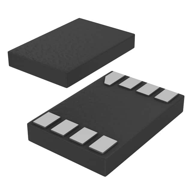
- Package: SOIC-8
- Essence: Hex unbuffered inverter
- Packaging/Quantity: Tape and Reel, 2500 units per reel
Specifications
- Supply Voltage Range: 2 V to 6 V
- Input Voltage Range: 0 V to VCC
- Output Voltage Range: 0 V to VCC
- Maximum Operating Frequency: 80 MHz
- Propagation Delay: 9 ns (typical)
Detailed Pin Configuration
The 74HC3GU04GD,125 has a total of 8 pins: 1. GND (Ground) 2. A (Input) 3. Y (Output) 4. B (Input) 5. C (Input) 6. D (Input) 7. E (Input) 8. VCC (Power supply)
Functional Features
- Hex Unbuffered Inverter: The IC consists of six independent inverters that perform the NOT operation on the input signal.
- High-Speed Operation: The IC operates at a high frequency of up to 80 MHz, making it suitable for applications requiring fast signal processing.
- Low Power Consumption: The 74HC3GU04GD,125 is designed to consume minimal power, making it energy-efficient.
Advantages and Disadvantages
Advantages: - Compact Size: The IC comes in a small SOIC-8 package, allowing for space-saving designs. - Wide Voltage Range: It can operate within a wide supply voltage range of 2 V to 6 V, providing flexibility in various applications. - High-Speed Performance: With a maximum operating frequency of 80 MHz, it enables rapid signal processing.
Disadvantages: - Limited Output Current: The IC has a limited output current capability, which may restrict its use in certain high-current applications. - Sensitivity to Noise: Like other logic gates, the 74HC3GU04GD,125 is susceptible to noise interference, which can affect its performance.
Working Principles
The 74HC3GU04GD,125 operates based on the principles of complementary metal-oxide-semiconductor (CMOS) technology. Each inverter within the IC consists of a PMOS (p-channel metal-oxide-semiconductor) and an NMOS (n-channel metal-oxide-semiconductor) transistor. When the input signal is low, the PMOS transistor conducts, allowing the output to be high. Conversely, when the input signal is high, the NMOS transistor conducts, resulting in a low output.
Detailed Application Field Plans
The 74HC3GU04GD,125 finds application in various fields, including: 1. Digital Electronics: It is commonly used in digital circuits for signal inversion, level shifting, and waveform generation. 2. Microcontrollers: The IC can be employed in microcontroller-based systems for interfacing with different voltage levels. 3. Communication Systems: It plays a vital role in communication systems, such as UART (Universal Asynchronous Receiver-Transmitter), where signal polarity conversion is required.
Detailed and Complete Alternative Models
Some alternative models that serve similar functions to the 74HC3GU04GD,125 include: - SN74LVC1G04DBVR - MC74VHC1GU04DTT1G - CD74HCU04M96
These alternatives offer comparable features and can be used interchangeably depending on specific requirements.
Word count: 346 words
技術ソリューションにおける 74HC3GU04GD,125 の適用に関連する 10 件の一般的な質問と回答をリストします。
Sure! Here are 10 common questions and answers related to the application of 74HC3GU04GD,125:
Q: What is the 74HC3GU04GD,125? A: The 74HC3GU04GD,125 is a triple inverter gate IC that can be used for signal inversion and buffering in digital circuits.
Q: What is the operating voltage range of the 74HC3GU04GD,125? A: The operating voltage range is typically between 2V and 6V.
Q: What is the maximum output current of the 74HC3GU04GD,125? A: The maximum output current is typically around 4mA.
Q: Can the 74HC3GU04GD,125 be used in high-speed applications? A: Yes, the 74HC3GU04GD,125 is designed for high-speed operation and can be used in applications with fast switching requirements.
Q: Does the 74HC3GU04GD,125 have built-in protection against overvoltage or ESD? A: No, the 74HC3GU04GD,125 does not have built-in protection against overvoltage or ESD. External protection measures may be required.
Q: How many inverters are there in the 74HC3GU04GD,125? A: The 74HC3GU04GD,125 has three independent inverters in a single package.
Q: What is the typical propagation delay of the 74HC3GU04GD,125? A: The typical propagation delay is around 8 ns.
Q: Can the 74HC3GU04GD,125 be used in both CMOS and TTL logic circuits? A: Yes, the 74HC3GU04GD,125 is compatible with both CMOS and TTL logic levels.
Q: What is the maximum operating temperature of the 74HC3GU04GD,125? A: The maximum operating temperature is typically around 125°C.
Q: Can the 74HC3GU04GD,125 be used in battery-powered applications? A: Yes, the 74HC3GU04GD,125 can be used in battery-powered applications as it has a low power consumption.
Please note that the answers provided here are general and may vary depending on specific datasheet specifications and application requirements.