

Encyclopedia Entry: 74AUP2G79DC-Q100H
Product Overview
Category
The 74AUP2G79DC-Q100H belongs to the category of integrated circuits (ICs), specifically digital logic gates.
Use
This product is primarily used for signal processing and logic operations in various electronic devices and systems.
Characteristics
- Low power consumption: The 74AUP2G79DC-Q100H is designed to operate with low power requirements, making it suitable for battery-powered applications.
- High-speed operation: This IC offers fast switching speeds, enabling efficient data processing.
- Small form factor: The compact size of this product allows for space-saving integration into electronic designs.
- Wide operating voltage range: The 74AUP2G79DC-Q100H can operate within a broad voltage range, enhancing its versatility.
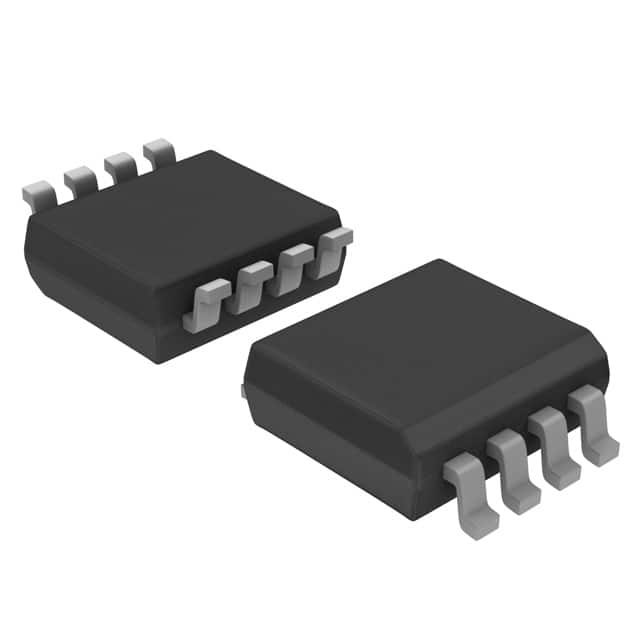
Package
The 74AUP2G79DC-Q100H is available in a small package, such as a dual flat no-lead (DFN) or thin small outline package (TSOP).
Essence
This IC serves as a fundamental building block for digital circuits, providing logical functions essential for data manipulation and control.
Packaging/Quantity
The 74AUP2G79DC-Q100H is typically sold in reels or tubes, containing a specific quantity of ICs per package. The exact quantity may vary depending on the supplier.
Specifications
- Supply voltage: 1.65V to 5.5V
- Operating temperature range: -40°C to +125°C
- Logic family: AUP
- Number of inputs: 2
- Number of outputs: 1
- Logic function: Dual positive-edge-triggered D-type flip-flop
Detailed Pin Configuration
The 74AUP2G79DC-Q100H features the following pin configuration:
+-----------------+
  D1 --|1              6|-- VCC
  D2 --|2   74AUP2G79   5|-- Q
 GND --|3              4|-- CLK
        +-----------------+
Functional Features
- Dual flip-flop: The 74AUP2G79DC-Q100H integrates two independent D-type flip-flops, allowing for simultaneous processing of multiple signals.
- Positive-edge-triggered: This IC responds to changes in input data at the rising edge of the clock signal, ensuring accurate and synchronized output.
- Asynchronous clear input: The presence of a clear input allows for immediate resetting of the flip-flop's state, providing flexibility in control.
Advantages and Disadvantages
Advantages
- Low power consumption enables energy-efficient operation.
- High-speed performance facilitates rapid data processing.
- Small form factor allows for compact integration into electronic designs.
- Wide operating voltage range enhances versatility.
Disadvantages
- Limited number of inputs and outputs may restrict complex circuit designs.
- Lack of additional advanced features compared to more specialized ICs.
Working Principles
The 74AUP2G79DC-Q100H operates based on the principles of digital logic. It utilizes positive-edge-triggered D-type flip-flops to store and manipulate binary data. The flip-flops respond to changes in the input data at the rising edge of the clock signal, updating the output accordingly. The asynchronous clear input provides a means to reset the flip-flop's state independently of the clock signal.
Detailed Application Field Plans
The 74AUP2G79DC-Q100H finds applications in various fields, including but not limited to: - Consumer electronics: Used in smartphones, tablets, and portable devices for signal processing and control functions. - Automotive systems: Integrated into automotive electronics for data manipulation and control in engine management, infotainment systems, and more. - Industrial automation: Employed in industrial control systems for logic operations and signal processing.
Detailed and Complete Alternative Models
- 74AUP2G79DC-Q100HX: Similar to the 74AUP2G79DC-Q100H but with extended temperature range (-55°C to +125°C).
- 74AUP2G79DC-Q100HL: Low-power variant of the 74AUP2G79DC-Q100H with further reduced power consumption.
- 74AUP2G79DC-Q100HT: High-speed version of the 74AUP2G79DC-Q100H with improved switching speeds.
These alternative models offer similar functionality while catering to specific requirements or constraints.
Word count: 550 words
技術ソリューションにおける 74AUP2G79DC-Q100H の適用に関連する 10 件の一般的な質問と回答をリストします。
Sure! Here are 10 common questions and answers related to the application of 74AUP2G79DC-Q100H in technical solutions:
Q: What is the 74AUP2G79DC-Q100H? A: The 74AUP2G79DC-Q100H is a dual positive-edge triggered D-type flip-flop with set and reset inputs.
Q: What is the operating voltage range for the 74AUP2G79DC-Q100H? A: The operating voltage range for this IC is from 0.8V to 3.6V.
Q: What is the maximum clock frequency supported by the 74AUP2G79DC-Q100H? A: The maximum clock frequency supported is typically around 400 MHz.
Q: Can I use the 74AUP2G79DC-Q100H in battery-powered applications? A: Yes, the low operating voltage range makes it suitable for battery-powered applications.
Q: Does the 74AUP2G79DC-Q100H have any built-in protection features? A: Yes, it has built-in ESD protection, making it more robust against electrostatic discharge.
Q: What is the typical power consumption of the 74AUP2G79DC-Q100H? A: The typical power consumption is very low, making it suitable for power-sensitive applications.
Q: Can I cascade multiple 74AUP2G79DC-Q100H flip-flops together? A: Yes, you can cascade multiple flip-flops to create larger registers or counters.
Q: Are there any specific timing requirements for the inputs of the 74AUP2G79DC-Q100H? A: Yes, the datasheet provides detailed timing diagrams and specifications for proper operation.
Q: Can I use the 74AUP2G79DC-Q100H in high-speed data transmission applications? A: While it can handle relatively high clock frequencies, it may not be suitable for very high-speed data transmission applications.
Q: Are there any recommended decoupling capacitors for the 74AUP2G79DC-Q100H? A: It is generally recommended to include decoupling capacitors near the power supply pins to ensure stable operation.
Please note that these answers are general and may vary depending on specific application requirements. Always refer to the datasheet and consult with an expert for accurate information.