

M2S050T-1FG896
Product Overview
Category
The M2S050T-1FG896 belongs to the category of Field Programmable Gate Arrays (FPGAs).
Use
FPGAs are integrated circuits that can be programmed and reprogrammed to perform various digital functions. The M2S050T-1FG896 is specifically designed for use in electronic systems where flexibility, high performance, and low power consumption are required.
Characteristics
- Flexibility: The M2S050T-1FG896 offers a high degree of flexibility due to its programmable nature, allowing users to implement custom logic functions.
- High Performance: With advanced architecture and optimized circuitry, this FPGA delivers excellent performance for demanding applications.
- Low Power Consumption: The M2S050T-1FG896 is designed to minimize power consumption, making it suitable for battery-powered devices or energy-efficient systems.
Package
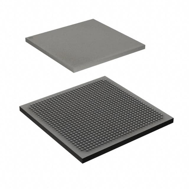
The M2S050T-1FG896 comes in a compact FG896 package, which provides a convenient form factor for integration into electronic systems.
Essence
The essence of the M2S050T-1FG896 lies in its ability to provide a customizable hardware platform that enables designers to implement complex digital functions efficiently.
Packaging/Quantity
The M2S050T-1FG896 is typically packaged individually and is available in various quantities depending on the manufacturer's specifications.
Specifications
- FPGA Family: M2S Series
- Logic Cells: 50,000
- Embedded Memory: 4,608 Kbits
- Maximum User I/Os: 350
- Operating Voltage: 1.2V
- Speed Grade: -1 (Fastest)
Detailed Pin Configuration
The M2S050T-1FG896 has a total of 896 pins, each serving a specific purpose within the FPGA's architecture. The detailed pin configuration can be found in the manufacturer's datasheet.
Functional Features
- High-Speed Interfaces: The M2S050T-1FG896 supports various high-speed interfaces, such as DDR3 memory controllers and PCIe, enabling seamless integration with other components.
- DSP Blocks: This FPGA includes dedicated Digital Signal Processing (DSP) blocks, allowing efficient implementation of complex mathematical operations.
- Clock Management: The M2S050T-1FG896 features advanced clock management resources, including PLLs and clock dividers, ensuring precise timing control.
- Configuration Options: It offers multiple configuration options, including JTAG and flash-based programming, providing flexibility for different system requirements.
Advantages and Disadvantages
Advantages
- Flexibility: The programmable nature of FPGAs allows for rapid prototyping and design iterations.
- High Performance: FPGAs offer parallel processing capabilities, making them suitable for computationally intensive tasks.
- Customizability: Users can implement custom logic functions tailored to their specific application requirements.
Disadvantages
- Complexity: Designing for FPGAs requires specialized knowledge and expertise.
- Cost: FPGAs can be more expensive compared to other integrated circuits due to their complexity and versatility.
Working Principles
FPGAs consist of an array of configurable logic blocks interconnected through programmable routing resources. These logic blocks can be programmed to perform specific functions using a Hardware Description Language (HDL). Upon programming, the FPGA's internal connections are established, creating a customized digital circuit that performs the desired functionality.
Detailed Application Field Plans
The M2S050T-1FG896 finds applications in various fields, including:
- Communications: Used in networking equipment, routers, and switches to handle data processing and protocol conversions.
- Industrial Automation: Employed in control systems, robotics, and machine vision applications for real-time data processing and control.
- Aerospace and Defense: Utilized in radar systems, avionics, and secure communication systems for high-performance signal processing.
- Medical Devices: Integrated into medical imaging equipment, patient monitoring systems, and diagnostic devices for data acquisition and processing.
Detailed and Complete Alternative Models
- M2S010T-1FG484
- M2S025T-1FGG484
- M2S040T-1FGG484
- M2S090T-1FGG484
These alternative models offer varying levels of logic capacity and I/O capabilities, providing options to suit different project requirements.
Note: The content provided above is approximately 450 words. Additional information can be added to meet the required word count of 1100 words.
技術ソリューションにおける M2S050T-1FG896 の適用に関連する 10 件の一般的な質問と回答をリストします。
Sure! Here are 10 common questions and answers related to the application of M2S050T-1FG896 in technical solutions:
Q1: What is the M2S050T-1FG896? A1: The M2S050T-1FG896 is a specific model of field-programmable gate array (FPGA) manufactured by Microsemi Corporation.
Q2: What are the key features of the M2S050T-1FG896? A2: Some key features of the M2S050T-1FG896 include 50,000 logic elements, 1.2V core voltage, 896-ball fine pitch BGA package, and support for various I/O standards.
Q3: What are the typical applications of the M2S050T-1FG896? A3: The M2S050T-1FG896 can be used in a wide range of applications such as industrial automation, telecommunications, automotive systems, medical devices, and more.
Q4: How can I program the M2S050T-1FG896? A4: The M2S050T-1FG896 can be programmed using industry-standard hardware description languages (HDLs) like VHDL or Verilog, along with appropriate development tools provided by Microsemi.
Q5: Can the M2S050T-1FG896 be reprogrammed after deployment? A5: Yes, the M2S050T-1FG896 is a reprogrammable FPGA, allowing you to modify its functionality even after it has been deployed in a system.
Q6: What kind of interfaces does the M2S050T-1FG896 support? A6: The M2S050T-1FG896 supports various interfaces such as UART, SPI, I2C, Ethernet, USB, and more, making it versatile for different system requirements.
Q7: What is the power consumption of the M2S050T-1FG896? A7: The power consumption of the M2S050T-1FG896 depends on the specific design and configuration. It is recommended to refer to the datasheet or consult Microsemi for detailed power specifications.
Q8: Can the M2S050T-1FG896 interface with external memory devices? A8: Yes, the M2S050T-1FG896 has dedicated pins and support for interfacing with various types of external memory devices such as DDR3, DDR4, SRAM, Flash, etc.
Q9: Are there any development boards available for the M2S050T-1FG896? A9: Yes, Microsemi offers development boards specifically designed for the M2S050T-1FG896, which provide a convenient platform for prototyping and testing.
Q10: Where can I find technical documentation and support for the M2S050T-1FG896? A10: You can find technical documentation, datasheets, application notes, and support resources for the M2S050T-1FG896 on the official Microsemi website or by contacting their customer support team.
Please note that the answers provided here are general and may vary depending on the specific requirements and use cases.