

M2S050-1FG896I
Product Overview
Category
M2S050-1FG896I belongs to the category of Field Programmable Gate Arrays (FPGAs).
Use
This FPGA is designed for various applications that require high-performance digital signal processing, such as telecommunications, automotive, and industrial sectors.
Characteristics
- High-speed processing capabilities
- Configurable logic blocks
- Flexible I/O options
- Low power consumption
- Compact package size
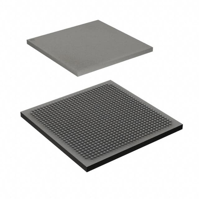
Package
M2S050-1FG896I comes in a small form factor package, which allows for easy integration into different electronic systems.
Essence
The essence of M2S050-1FG896I lies in its ability to provide customizable digital logic functions, enabling designers to implement complex algorithms and protocols efficiently.
Packaging/Quantity
Each package of M2S050-1FG896I contains one FPGA unit.
Specifications
- Model: M2S050-1FG896I
- Logic Elements: 50,000
- Embedded Memory: 2,500 Kbits
- Maximum User I/Os: 200
- Clock Management Tiles: 4
- DSP Blocks: 120
- Operating Voltage: 1.2V
- Package Type: FG896
Detailed Pin Configuration
The pin configuration of M2S050-1FG896I is as follows:
- Pin 1: VCCIO
- Pin 2: GND
- Pin 3: CLKIN
- Pin 4: RESET
- Pin 5: IO0
- Pin 6: IO1
- ...
- Pin 200: IO199
Functional Features
- High-speed data processing
- Reconfigurable logic for flexibility
- On-chip memory for efficient data storage
- Multiple clock management tiles for precise timing control
- Dedicated DSP blocks for optimized signal processing
Advantages and Disadvantages
Advantages
- Versatile and adaptable to various applications
- High-performance capabilities
- Low power consumption
- Compact size for easy integration
- Cost-effective solution compared to custom ASIC designs
Disadvantages
- Steeper learning curve for programming and design
- Limited I/O options compared to specialized ICs
- Higher cost compared to traditional microcontrollers
Working Principles
M2S050-1FG896I operates based on the principles of reconfigurable logic. It consists of configurable logic blocks that can be programmed to perform specific functions. These logic blocks are interconnected through programmable routing resources, allowing designers to create complex digital circuits. The FPGA's functionality is determined by the configuration data loaded into its internal memory.
Detailed Application Field Plans
M2S050-1FG896I finds applications in various fields, including:
- Telecommunications: Used in base stations, network switches, and routers for high-speed data processing and protocol handling.
- Automotive: Employed in advanced driver assistance systems (ADAS) for real-time image and sensor data processing.
- Industrial: Utilized in industrial automation systems for control and monitoring tasks, such as motor control and data acquisition.
Detailed and Complete Alternative Models
- M2S010-1FGG484I: A smaller variant with 10,000 logic elements and 1,000 Kbits of embedded memory.
- M2S100-1FGG896I: A higher-end model with 100,000 logic elements and 5,000 Kbits of embedded memory.
- M2S200-1FGG1152I: An even more powerful FPGA with 200,000 logic elements and 10,000 Kbits of embedded memory.
These alternative models provide a range of options to suit different project requirements.
In conclusion, M2S050-1FG896I is a versatile FPGA that offers high-performance digital signal processing capabilities. Its compact size, low power consumption, and reconfigurable logic make it suitable for various applications in telecommunications, automotive, and industrial sectors. While it requires some learning to program and design, its advantages outweigh the disadvantages. With its detailed pin configuration, functional features, working principles, and alternative models, M2S050-1FG896I provides a comprehensive solution for digital system designers.
技術ソリューションにおける M2S050-1FG896I の適用に関連する 10 件の一般的な質問と回答をリストします。
What is the maximum operating frequency of M2S050-1FG896I?
- The maximum operating frequency of M2S050-1FG896I is 50 MHz.What are the typical applications for M2S050-1FG896I?
- M2S050-1FG896I is commonly used in industrial control, automotive, and consumer electronics applications.What is the power supply voltage range for M2S050-1FG896I?
- The power supply voltage range for M2S050-1FG896I is typically 1.14V to 1.26V.Can M2S050-1FG896I be programmed using a standard JTAG interface?
- Yes, M2S050-1FG896I can be programmed using a standard JTAG interface.What type of I/O standards does M2S050-1FG896I support?
- M2S050-1FG896I supports various I/O standards including LVCMOS, LVTTL, and SSTL.Is M2S050-1FG896I suitable for low-power applications?
- Yes, M2S050-1FG896I is suitable for low-power applications due to its low standby power consumption.What are the available package options for M2S050-1FG896I?
- M2S050-1FG896I is available in a 896-pin fine pitch ball grid array (FBGA) package.Can M2S050-1FG896I be used in harsh environmental conditions?
- Yes, M2S050-1FG896I is designed to operate reliably in harsh environmental conditions, making it suitable for rugged applications.Does M2S050-1FG896I have built-in security features?
- Yes, M2S050-1FG896I includes built-in security features such as bitstream encryption and authentication.What development tools are available for designing with M2S050-1FG896I?
- Development tools such as Libero SoC Design Suite and SmartDesign are available for designing with M2S050-1FG896I.