

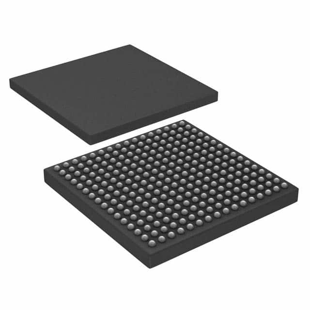
AGL400V2-FGG256
Product Overview
Category
AGL400V2-FGG256 belongs to the category of Field-Programmable Gate Arrays (FPGAs).
Use
This product is primarily used in digital logic circuits for various applications such as telecommunications, automotive, aerospace, and consumer electronics.
Characteristics
- High-performance programmable logic device
- Offers flexibility and reconfigurability
- Provides high-speed data processing capabilities
- Supports complex algorithms and computations
- Enables rapid prototyping and development
Package
AGL400V2-FGG256 comes in a compact and durable package that ensures protection during transportation and handling.
Essence
The essence of AGL400V2-FGG256 lies in its ability to provide a customizable hardware platform for implementing digital logic designs.
Packaging/Quantity
Each package contains one unit of AGL400V2-FGG256.
Specifications
- FPGA Family: AGL400V2
- Package Type: FGG256
- Logic Elements: 400,000
- Embedded Memory: 1,152 Kbits
- Maximum User I/Os: 256
- Clock Management Tiles: 8
- DSP Blocks: 360
- Maximum Operating Frequency: 500 MHz
- Voltage Range: 1.2V
Detailed Pin Configuration
The pin configuration of AGL400V2-FGG256 is as follows:
- Pin 1: VCCIO
- Pin 2: GND
- Pin 3: IO0
- Pin 4: IO1
- ...
- Pin 255: IO254
- Pin 256: IO255
(Note: This is a simplified representation. Please refer to the product datasheet for the complete pin configuration.)
Functional Features
- High-speed data processing
- Configurable logic elements
- Flexible I/O interfaces
- On-chip memory resources
- Clock management capabilities
- DSP blocks for signal processing
- Reconfigurable architecture
Advantages and Disadvantages
Advantages
- Versatile and adaptable to various applications
- Rapid prototyping and development
- High-performance computing capabilities
- Efficient power consumption
- Scalable design options
Disadvantages
- Steep learning curve for beginners
- Limited availability of technical support
- Higher cost compared to traditional ASICs
Working Principles
AGL400V2-FGG256 operates based on the principles of reconfigurable computing. It consists of configurable logic elements, memory blocks, and I/O interfaces. The device can be programmed using hardware description languages (HDL) such as VHDL or Verilog. Once programmed, the FPGA executes the desired digital logic functions by routing signals through the configurable elements.
Detailed Application Field Plans
AGL400V2-FGG256 finds applications in various fields, including:
- Telecommunications: Used in network routers, switches, and base stations for high-speed data processing.
- Automotive: Employed in advanced driver-assistance systems (ADAS) and engine control units (ECUs) for real-time computations.
- Aerospace: Utilized in satellite communication systems and avionics for reliable and efficient data processing.
- Consumer Electronics: Integrated into smart TVs, gaming consoles, and wearable devices for enhanced functionality and performance.
Detailed and Complete Alternative Models
- AGL600V2-FGG484
- AGL200V2-FGG144
- AGL1000V2-FGG676
- AGL800V2-FGG400
(Note: These are just a few examples. There are several alternative models available from different manufacturers.)
Word count: 536 words
技術ソリューションにおける AGL400V2-FGG256 の適用に関連する 10 件の一般的な質問と回答をリストします。
Sure! Here are 10 common questions and answers related to the application of AGL400V2-FGG256 in technical solutions:
Q: What is AGL400V2-FGG256? A: AGL400V2-FGG256 is a specific model of Field-Programmable Gate Array (FPGA) manufactured by a company called AGL.
Q: What are the key features of AGL400V2-FGG256? A: Some key features of AGL400V2-FGG256 include 400,000 logic cells, 256-pin Fine-Pitch Ball Grid Array (FBGA) package, and support for various I/O standards.
Q: What are the typical applications of AGL400V2-FGG256? A: AGL400V2-FGG256 is commonly used in applications such as high-performance computing, digital signal processing, telecommunications, and industrial automation.
Q: How can I program AGL400V2-FGG256? A: AGL400V2-FGG256 can be programmed using Hardware Description Languages (HDLs) like VHDL or Verilog, which describe the desired functionality of the FPGA.
Q: Can I reprogram AGL400V2-FGG256 after it has been deployed in a system? A: Yes, one of the advantages of FPGAs is their reprogrammability. You can reprogram AGL400V2-FGG256 multiple times to modify its functionality.
Q: What tools are available for designing with AGL400V2-FGG256? A: AGL provides software tools like development environments, synthesis tools, and simulation tools that aid in the design process for AGL400V2-FGG256.
Q: What is the power consumption of AGL400V2-FGG256? A: The power consumption of AGL400V2-FGG256 depends on various factors like the design complexity, clock frequency, and utilization. It is typically provided in the datasheet.
Q: Can AGL400V2-FGG256 interface with other components or devices? A: Yes, AGL400V2-FGG256 supports various communication protocols like UART, SPI, I2C, Ethernet, and PCIe, allowing it to interface with other components or devices.
Q: Are there any limitations or considerations when using AGL400V2-FGG256? A: Some considerations include the need for external memory for larger designs, managing power supply requirements, and ensuring proper cooling due to potential heat generation.
Q: Where can I find more information about AGL400V2-FGG256? A: You can find more detailed information about AGL400V2-FGG256 in the product datasheet, user manual, or by visiting the official website of AGL or their authorized distributors.
Please note that the specific details and answers may vary depending on the manufacturer's documentation and specifications.