

A54SX32A-1FG144
Product Overview
Category
The A54SX32A-1FG144 belongs to the category of Field Programmable Gate Arrays (FPGAs).
Use
FPGAs are integrated circuits that can be programmed and reprogrammed to perform various digital functions. The A54SX32A-1FG144 is specifically designed for applications requiring high-performance logic integration.
Characteristics
- High-performance FPGA with 54,000 system gates
- Advanced architecture for efficient logic implementation
- Flexible and reconfigurable design
- Low power consumption
- Fast signal processing capabilities
Package
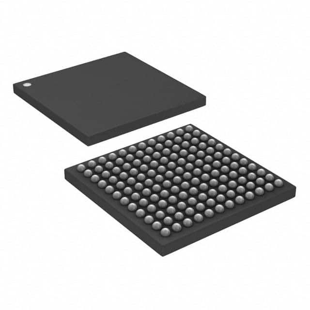
The A54SX32A-1FG144 comes in a 144-pin Fine-Pitch Ball Grid Array (FBGA) package.
Essence
The essence of the A54SX32A-1FG144 lies in its ability to provide a versatile and customizable solution for complex digital circuit designs.
Packaging/Quantity
The A54SX32A-1FG144 is typically packaged individually and is available in various quantities depending on the manufacturer's specifications.
Specifications
- System Gates: 54,000
- Logic Cells: 32,768
- I/O Pins: 144
- Operating Voltage: 3.3V
- Maximum Frequency: 200 MHz
- Embedded Memory: Up to 2,048 Kbits
- Programmable Interconnects: 1,152
Detailed Pin Configuration
The A54SX32A-1FG144 has 144 pins, each serving a specific purpose in the overall functionality of the FPGA. The pin configuration includes dedicated input/output pins, clock pins, power supply pins, and configuration pins. For a detailed pin configuration diagram, please refer to the manufacturer's datasheet.
Functional Features
- High-speed data processing capabilities
- Configurable logic blocks for flexible design implementation
- On-chip memory for efficient data storage and retrieval
- Built-in clock management resources for precise timing control
- Support for various communication protocols and interfaces
- Reconfigurable architecture for easy system upgrades
Advantages and Disadvantages
Advantages
- Versatile and customizable solution for complex digital designs
- High-performance logic integration
- Low power consumption compared to traditional ASICs
- Faster time-to-market due to reprogrammability
- Cost-effective for low to medium volume production
Disadvantages
- Limited performance compared to dedicated application-specific integrated circuits (ASICs)
- Higher power consumption compared to specialized ASICs
- Design complexity may require advanced programming skills
- Relatively higher cost per unit compared to standard logic gates
Working Principles
The A54SX32A-1FG144 operates based on the principles of configurable logic. It consists of a matrix of programmable logic cells interconnected through programmable interconnects. The user can program the FPGA using hardware description languages (HDL) or graphical tools to define the desired functionality. Once programmed, the FPGA executes the specified logic operations, providing the desired output based on the input signals.
Detailed Application Field Plans
The A54SX32A-1FG144 finds applications in various fields, including:
- Telecommunications: Used in base stations, network switches, and routers for high-speed data processing and protocol handling.
- Industrial Automation: Employed in control systems, robotics, and machine vision applications for real-time data processing and control.
- Automotive: Utilized in advanced driver assistance systems (ADAS), infotainment systems, and engine control units (ECUs) for enhanced performance and functionality.
- Aerospace and Defense: Integrated into avionics systems, radar systems, and satellite communication equipment for reliable and high-performance signal processing.
- Medical Devices: Applied in medical imaging systems, patient monitoring devices, and laboratory equipment for efficient data processing and analysis.
Detailed and Complete Alternative Models
- A54SX16A-1FG144: Similar to the A54SX32A-1FG144 but with 16,000 system gates.
- A54SX64A-1FG144: Higher-end model with 64,000 system gates for more complex designs.
- A54SX128A-1FG144: Advanced version with 128,000 system gates for larger-scale applications.
These alternative models provide varying levels of logic integration and can be chosen based on specific project requirements.
In conclusion, the A54SX32A-1FG144 is a high-performance FPGA that offers flexibility, reconfigurability, and efficient logic implementation. It finds applications in diverse fields, providing a versatile solution for complex digital circuit designs.
技術ソリューションにおける A54SX32A-1FG144 の適用に関連する 10 件の一般的な質問と回答をリストします。
Sure! Here are 10 common questions and answers related to the application of A54SX32A-1FG144 in technical solutions:
Q1: What is the A54SX32A-1FG144? A1: The A54SX32A-1FG144 is a specific model of field-programmable gate array (FPGA) manufactured by Microsemi Corporation.
Q2: What is an FPGA? A2: An FPGA is an integrated circuit that can be programmed after manufacturing to perform various digital functions, making it highly flexible for different applications.
Q3: What are the key features of the A54SX32A-1FG144? A3: The A54SX32A-1FG144 offers 54,000 system gates, 32,768 macrocells, and 144-pin FineLine BGA packaging. It also supports various I/O standards and has embedded memory blocks.
Q4: What are some typical applications of the A54SX32A-1FG144? A4: The A54SX32A-1FG144 can be used in a wide range of applications, including telecommunications, industrial automation, automotive electronics, medical devices, and more.
Q5: How can I program the A54SX32A-1FG144? A5: The A54SX32A-1FG144 can be programmed using hardware description languages (HDLs) such as VHDL or Verilog, which allow you to describe the desired functionality of the FPGA.
Q6: Can the A54SX32A-1FG144 be reprogrammed? A6: Yes, the A54SX32A-1FG144 is a reprogrammable FPGA, meaning you can change its functionality by reprogramming it with new designs as needed.
Q7: What tools are available for programming and configuring the A54SX32A-1FG144? A7: Microsemi provides software tools like Libero SoC Design Suite, which includes design entry, synthesis, simulation, place-and-route, and programming capabilities for their FPGAs.
Q8: What are the power requirements for the A54SX32A-1FG144? A8: The power requirements for the A54SX32A-1FG144 can vary depending on the specific application and configuration. It is important to consult the datasheet and reference designs provided by Microsemi for accurate power estimation.
Q9: Are there any limitations or considerations when using the A54SX32A-1FG144? A9: Some considerations include I/O voltage compatibility, thermal management, and ensuring proper signal integrity. It is recommended to refer to the datasheet and application notes for detailed guidelines.
Q10: Where can I find additional resources and support for the A54SX32A-1FG144? A10: Microsemi's website provides documentation, application notes, reference designs, and technical support for their FPGAs, including the A54SX32A-1FG144. You can also reach out to their customer support team for further assistance.