

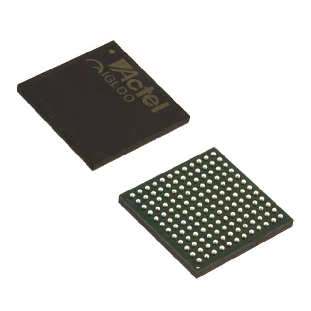
A54SX08A-FGG144
Product Overview
Category
The A54SX08A-FGG144 belongs to the category of Field-Programmable Gate Arrays (FPGAs).
Use
FPGAs are integrated circuits that can be programmed and reprogrammed to perform various digital functions. The A54SX08A-FGG144 is specifically designed for applications requiring high-performance logic integration.
Characteristics
- High-performance logic integration
- Programmable and reprogrammable functionality
- Flexible and customizable design options
Package
The A54SX08A-FGG144 comes in a compact Fine-Pitch Ball Grid Array (FBGA) package.
Essence
The essence of the A54SX08A-FGG144 lies in its ability to provide a versatile and configurable platform for implementing complex digital systems.
Packaging/Quantity
The A54SX08A-FGG144 is typically packaged individually and is available in varying quantities depending on the manufacturer's specifications.
Specifications
- Logic Elements: 8,000
- Maximum Number of User I/Os: 144
- Block RAM: 288 Kbits
- Clock Management Tiles: 4
- Maximum User Flash Memory: 1,152 Kbits
- Operating Voltage: 3.3V
Detailed Pin Configuration
The A54SX08A-FGG144 has a total of 144 pins, each serving a specific purpose in the FPGA's operation. For a detailed pin configuration diagram, please refer to the manufacturer's datasheet.
Functional Features
- High-speed performance
- Configurable logic blocks
- Dedicated clock management resources
- On-chip memory blocks
- Built-in programmable interconnects
Advantages and Disadvantages
Advantages
- Flexibility in design and customization
- Rapid prototyping and development
- Reconfigurability for future updates
- High-performance computing capabilities
Disadvantages
- Higher power consumption compared to fixed-function ASICs
- Longer development time compared to off-the-shelf solutions
- Limited availability of specialized technical expertise
Working Principles
The A54SX08A-FGG144 operates based on the principles of reconfigurable computing. It consists of a matrix of configurable logic blocks interconnected through programmable interconnects. The FPGA can be programmed using Hardware Description Languages (HDL) such as VHDL or Verilog, allowing users to define the desired functionality and behavior of the digital system.
Detailed Application Field Plans
The A54SX08A-FGG144 finds applications in various fields, including but not limited to: - Telecommunications - Industrial automation - Aerospace and defense - Medical devices - Automotive electronics
Detailed and Complete Alternative Models
- A54SX16A-FGG484
- A54SX32A-FGG484
- A54SX72A-FGG484
- A54SX16A-TQG100
- A54SX32A-TQG100
These alternative models offer different configurations and pin counts to cater to specific project requirements.
In conclusion, the A54SX08A-FGG144 is a high-performance FPGA that provides flexibility, configurability, and rapid prototyping capabilities. Its wide range of applications and availability of alternative models make it a versatile choice for digital system implementation.
技術ソリューションにおける A54SX08A-FGG144 の適用に関連する 10 件の一般的な質問と回答をリストします。
Sure! Here are 10 common questions and answers related to the application of A54SX08A-FGG144 in technical solutions:
Q: What is A54SX08A-FGG144? A: A54SX08A-FGG144 is a specific model of field-programmable gate array (FPGA) manufactured by Microsemi Corporation.
Q: What are the key features of A54SX08A-FGG144? A: Some key features of A54SX08A-FGG144 include 54,000 system gates, 8,192 macrocells, 144-pin FineLine BGA package, and support for various I/O standards.
Q: What are the typical applications of A54SX08A-FGG144? A: A54SX08A-FGG144 is commonly used in applications such as telecommunications, industrial automation, medical devices, aerospace, and defense.
Q: How can I program A54SX08A-FGG144? A: A54SX08A-FGG144 can be programmed using industry-standard hardware description languages (HDLs) like VHDL or Verilog, along with appropriate development tools provided by Microsemi.
Q: Can A54SX08A-FGG144 be reprogrammed after deployment? A: Yes, A54SX08A-FGG144 is a reprogrammable FPGA, allowing you to modify its functionality even after it has been deployed in a system.
Q: What voltage levels does A54SX08A-FGG144 support? A: A54SX08A-FGG144 supports various voltage levels, including 3.3V, 2.5V, and 1.8V, making it compatible with a wide range of systems.
Q: Does A54SX08A-FGG144 have built-in security features? A: Yes, A54SX08A-FGG144 includes security features like bitstream encryption and tamper detection to protect the intellectual property programmed into the FPGA.
Q: Can A54SX08A-FGG144 interface with other components or devices? A: Yes, A54SX08A-FGG144 supports various communication interfaces such as SPI, I2C, UART, and GPIOs, allowing it to interface with other components or devices in a system.
Q: What is the power consumption of A54SX08A-FGG144? A: The power consumption of A54SX08A-FGG144 depends on the specific design and configuration implemented on the FPGA. It is recommended to refer to the datasheet for detailed power specifications.
Q: Are there any development kits available for A54SX08A-FGG144? A: Yes, Microsemi offers development kits that include the necessary hardware and software tools to facilitate the design and programming of A54SX08A-FGG144-based solutions.
Please note that the answers provided here are general and may vary depending on the specific requirements and implementation of the technical solution.