

A42MX09-1PL84I
Product Overview
Category
The A42MX09-1PL84I belongs to the category of programmable logic devices (PLDs).
Use
This PLD is designed for use in various electronic systems where programmable logic functionality is required.
Characteristics
- High-performance programmable logic device
- Offers flexibility and versatility in system design
- Provides efficient implementation of complex digital circuits
- Supports a wide range of applications
Package
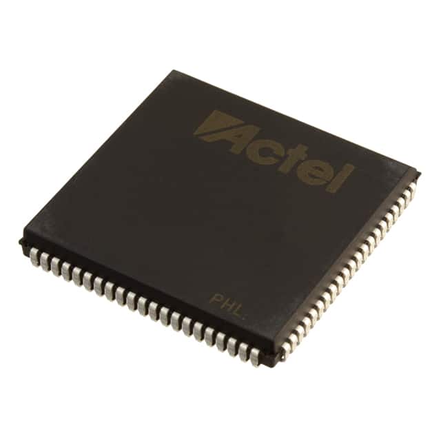
The A42MX09-1PL84I comes in a compact 84-pin plastic leaded chip carrier (PLCC) package.
Essence
The essence of this product lies in its ability to provide reconfigurable logic functions, allowing designers to customize their digital circuits according to specific requirements.
Packaging/Quantity
Each package contains one A42MX09-1PL84I programmable logic device.
Specifications
- Logic Cells: 9,600
- Maximum User I/Os: 68
- Flip-Flops: 4,800
- Maximum Frequency: 100 MHz
- Operating Voltage: 3.3V
- Programmable Interconnect Points: 8,000
- Embedded Block RAM: 144 Kbits
- JTAG Boundary Scan Support: Yes
Detailed Pin Configuration
The A42MX09-1PL84I has a total of 84 pins, each serving a specific function within the device. The detailed pin configuration can be found in the manufacturer's datasheet.
Functional Features
- High-density programmable logic device
- Flexible interconnect structure for efficient routing
- Embedded memory blocks for data storage
- JTAG boundary scan support for easy testing and debugging
- Low power consumption
- Fast performance with high-speed clocking capabilities
Advantages and Disadvantages
Advantages
- Versatile and customizable for various applications
- High logic capacity for complex designs
- Efficient interconnect structure for optimal routing
- Embedded memory blocks enhance functionality
- JTAG boundary scan support simplifies testing and debugging
Disadvantages
- Limited number of user I/Os compared to some other PLDs
- Relatively higher cost compared to simpler programmable logic devices
Working Principles
The A42MX09-1PL84I operates based on the principles of programmable logic. It consists of configurable logic blocks, interconnect resources, and embedded memory blocks. The device can be programmed using hardware description languages (HDL) or design entry tools to define the desired logic functions and interconnections. Once programmed, the device executes the specified logic operations, enabling the desired functionality.
Detailed Application Field Plans
The A42MX09-1PL84I finds applications in various fields, including but not limited to: - Industrial automation - Telecommunications - Automotive electronics - Consumer electronics - Medical devices - Aerospace and defense systems
Detailed and Complete Alternative Models
- A42MX16-1PQ100I
- A42MX24-1PLG84I
- A42MX36-1PQ160I
- A42MX49-1PLG84I
- A42MX75-1PLG84I
These alternative models offer different logic capacities, pin configurations, and package options to cater to diverse design requirements.
Note: The above information is based on the available documentation and specifications provided by the manufacturer. It is recommended to refer to the official datasheet for the most accurate and up-to-date details.
技術ソリューションにおける A42MX09-1PL84I の適用に関連する 10 件の一般的な質問と回答をリストします。
Sure! Here are 10 common questions and answers related to the application of A42MX09-1PL84I in technical solutions:
Q1: What is the A42MX09-1PL84I? A1: The A42MX09-1PL84I is a specific model of programmable logic device (PLD) manufactured by Microsemi Corporation.
Q2: What are the key features of the A42MX09-1PL84I? A2: The A42MX09-1PL84I offers 9,600 usable gates, 384 macrocells, and operates at a maximum frequency of 100 MHz. It also has 84 pins in a plastic leaded chip carrier (PLCC) package.
Q3: What are some typical applications of the A42MX09-1PL84I? A3: The A42MX09-1PL84I can be used in various technical solutions such as industrial control systems, telecommunications equipment, automotive electronics, and medical devices.
Q4: How does the A42MX09-1PL84I differ from other PLDs? A4: The A42MX09-1PL84I stands out due to its low power consumption, high performance, and flexible architecture that allows for efficient implementation of complex digital designs.
Q5: What development tools are available for programming the A42MX09-1PL84I? A5: Microsemi provides a range of development tools, including software like Libero SoC Design Suite and programming hardware like FlashPro programmer, to facilitate programming and configuration of the A42MX09-1PL84I.
Q6: Can the A42MX09-1PL84I be reprogrammed after deployment? A6: Yes, the A42MX09-1PL84I supports in-system programmability, allowing for reprogramming of the device even after it has been deployed in a system.
Q7: What are the voltage requirements for the A42MX09-1PL84I? A7: The A42MX09-1PL84I operates at a supply voltage range of 3.0V to 3.6V.
Q8: Is the A42MX09-1PL84I compatible with other PLDs or microcontrollers? A8: Yes, the A42MX09-1PL84I can be integrated with other PLDs, microcontrollers, or digital components through various interfaces like GPIOs, SPI, I2C, and UART.
Q9: Can the A42MX09-1PL84I handle analog signals? A9: No, the A42MX09-1PL84I is a digital device and does not directly process analog signals. However, it can interface with external analog-to-digital converters (ADCs) or digital-to-analog converters (DACs) for analog signal processing.
Q10: Where can I find more information about the A42MX09-1PL84I? A10: You can refer to the official documentation provided by Microsemi, including datasheets, application notes, and user guides, for detailed information about the A42MX09-1PL84I and its application in technical solutions.
Please note that the answers provided here are general and may vary depending on specific use cases and requirements.