

A3P400-FGG144I
Product Overview
Category
The A3P400-FGG144I belongs to the category of programmable logic devices (PLDs).
Use
This device is primarily used for digital circuit design and implementation. It offers a flexible and customizable solution for various applications.
Characteristics
- Programmable: The A3P400-FGG144I can be programmed to perform specific functions based on user requirements.
- High Integration: It integrates multiple logic gates, flip-flops, and other components into a single chip.
- Reconfigurable: The device can be reprogrammed multiple times, allowing for design modifications and updates.
- Low Power Consumption: The A3P400-FGG144I is designed to operate efficiently with minimal power consumption.
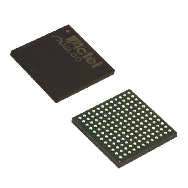
Package
The A3P400-FGG144I comes in a compact and durable package that ensures protection during handling and transportation.
Essence
The essence of the A3P400-FGG144I lies in its ability to provide a versatile and customizable solution for digital circuit design.
Packaging/Quantity
The device is typically packaged individually and is available in various quantities depending on customer requirements.
Specifications
- Model: A3P400-FGG144I
- Package Type: FGG144I
- Logic Cells: 400
- I/O Pins: 144
- Operating Voltage: 3.3V
- Speed Grade: Standard
Detailed Pin Configuration
The A3P400-FGG144I has a total of 144 pins, each serving a specific purpose in the circuit design. The pin configuration is as follows:
(Pin Number) - (Pin Name) 1 - VCCIO 2 - GND 3 - IO0 4 - IO1 5 - IO2 ... 144 - IO143
Functional Features
- Flexible Functionality: The A3P400-FGG144I can be programmed to perform a wide range of functions, making it suitable for diverse applications.
- High-Speed Operation: The device offers fast processing capabilities, enabling efficient execution of complex digital circuits.
- On-Chip Memory: It includes built-in memory elements that can store data and configuration settings.
- I/O Flexibility: The A3P400-FGG144I provides a sufficient number of I/O pins for interfacing with external devices.
Advantages and Disadvantages
Advantages
- Customizability: The device allows users to tailor the circuit design according to their specific requirements.
- Cost-Effective: Programmable logic devices eliminate the need for custom-designed integrated circuits, reducing development costs.
- Time-Saving: The reprogrammable nature of the A3P400-FGG144I enables faster prototyping and design iterations.
Disadvantages
- Limited Complexity: PLDs have certain limitations in terms of the complexity of circuits they can handle compared to application-specific integrated circuits (ASICs).
- Power Consumption: While efforts have been made to reduce power consumption, PLDs still consume more power compared to ASICs optimized for specific tasks.
Working Principles
The A3P400-FGG144I operates based on the principles of programmable logic. It consists of configurable logic blocks (CLBs), interconnect resources, and input/output blocks. The CLBs contain look-up tables (LUTs) that can be programmed to implement desired logic functions. The interconnect resources facilitate the routing of signals between different components, while the input/output blocks provide interfaces for external connections.
Detailed Application Field Plans
The A3P400-FGG144I finds applications in various fields, including:
- Industrial Automation: It can be used to control and monitor processes in manufacturing plants.
- Communication Systems: The device enables the implementation of digital signal processing algorithms in communication systems.
- Automotive Electronics: It can be utilized for designing control systems in vehicles, such as engine management and driver assistance systems.
- Consumer Electronics: The A3P400-FGG144I is suitable for applications like gaming consoles, home automation, and multimedia devices.
Detailed and Complete Alternative Models
- A3P1000-FG144I: This model offers a higher logic capacity and more I/O pins compared to the A3P400-FGG144I.
- A3P600-FGG144I: With a lower logic capacity, this model provides a cost-effective alternative for less complex designs.
- A3P250-FG144I: This model offers a smaller form factor and reduced power consumption, making it suitable for portable devices.
These alternative models provide options with varying capabilities to cater to different design requirements.
Word count: 560 words
技術ソリューションにおける A3P400-FGG144I の適用に関連する 10 件の一般的な質問と回答をリストします。
Sure! Here are 10 common questions and answers related to the application of A3P400-FGG144I in technical solutions:
1. What is the A3P400-FGG144I? - The A3P400-FGG144I is a specific model of FPGA (Field-Programmable Gate Array) manufactured by Microsemi.
2. What is an FPGA? - An FPGA is a type of integrated circuit that can be programmed after manufacturing to perform specific functions, making it highly versatile for various technical applications.
3. What are the key features of the A3P400-FGG144I? - The A3P400-FGG144I features 400,000 system gates, 4,608 logic elements, 64 I/O pins, and operates at a maximum frequency of 250 MHz.
4. What are some typical applications of the A3P400-FGG144I? - The A3P400-FGG144I is commonly used in applications such as industrial automation, robotics, telecommunications, medical devices, and automotive systems.
5. How can I program the A3P400-FGG144I? - The A3P400-FGG144I can be programmed using hardware description languages (HDLs) like VHDL or Verilog, which allow you to define the desired functionality of the FPGA.
6. Can I reprogram the A3P400-FGG144I multiple times? - Yes, the A3P400-FGG144I is a reprogrammable FPGA, meaning you can change its programming multiple times to adapt to different requirements.
7. What development tools are available for working with the A3P400-FGG144I? - Microsemi provides Libero SoC Design Suite, which includes software tools for designing, simulating, and programming the A3P400-FGG144I.
8. What is the power consumption of the A3P400-FGG144I? - The power consumption of the A3P400-FGG144I depends on the specific design and usage scenario. It is recommended to refer to the datasheet for detailed power specifications.
9. Can I interface the A3P400-FGG144I with other components or devices? - Yes, the A3P400-FGG144I supports various communication protocols such as SPI, I2C, UART, and GPIOs, allowing you to interface it with other components or devices in your system.
10. Are there any limitations or considerations when using the A3P400-FGG144I? - Some considerations include understanding the FPGA's resource limitations, ensuring proper power supply and cooling, and carefully designing the circuitry to avoid signal integrity issues. It is also important to follow the manufacturer's guidelines and recommendations for optimal performance and reliability.
Please note that these answers are general and may vary depending on the specific requirements and context of your technical solution.