

A3P250L-FGG144I
Product Overview
Category
The A3P250L-FGG144I belongs to the category of Field-Programmable Gate Arrays (FPGAs).
Use
This product is primarily used in digital logic circuits for various applications such as telecommunications, automotive, industrial automation, and consumer electronics.
Characteristics
- High-performance FPGA with advanced features
- Low power consumption
- Flexible and reprogrammable design
- Integration of multiple functions on a single chip
- High-speed data processing capabilities
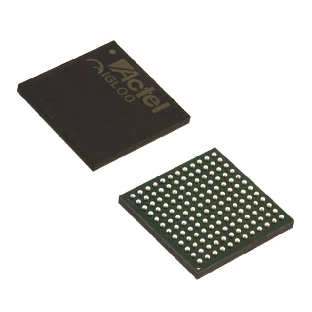
Package
The A3P250L-FGG144I comes in a compact and durable package that ensures protection during transportation and handling. The package is designed to withstand harsh environmental conditions.
Essence
The essence of the A3P250L-FGG144I lies in its ability to provide a customizable and versatile solution for complex digital circuit designs. It offers a high level of integration and performance while maintaining low power consumption.
Packaging/Quantity
Each package of A3P250L-FGG144I contains one unit of the FPGA. The quantity can vary depending on the specific requirements of the customer.
Specifications
- FPGA Family: A3P
- Logic Elements: 250,000
- Number of I/O Pins: 144
- Package Type: FGG144I
- Operating Voltage: 1.2V
- Maximum Frequency: 500 MHz
- Configuration Memory: Flash-based
Detailed Pin Configuration
The A3P250L-FGG144I has 144 pins, each serving a specific purpose in the overall functionality of the FPGA. The pin configuration includes input/output pins, clock pins, power supply pins, and configuration pins. For a detailed pin configuration diagram, please refer to the product datasheet.
Functional Features
- High-speed data processing capabilities
- Configurable logic elements for custom circuit designs
- On-chip memory blocks for efficient data storage
- Built-in clock management resources
- Support for various communication protocols
- Flexible I/O interfaces for seamless integration with external devices
Advantages and Disadvantages
Advantages
- Versatile and customizable design
- High-performance capabilities
- Low power consumption
- Compact package size
- Wide range of application possibilities
Disadvantages
- Steep learning curve for beginners
- Limited availability of technical support
- Higher cost compared to traditional logic circuits
Working Principles
The A3P250L-FGG144I operates based on the principles of reconfigurable digital logic. It consists of a matrix of configurable logic elements interconnected through programmable routing resources. The FPGA can be programmed using Hardware Description Languages (HDL) such as VHDL or Verilog, allowing designers to create complex digital circuits.
Detailed Application Field Plans
The A3P250L-FGG144I finds applications in various fields, including:
- Telecommunications: Used in network routers, switches, and base stations for high-speed data processing and protocol handling.
- Automotive: Employed in automotive control systems, infotainment systems, and driver assistance modules for enhanced functionality and performance.
- Industrial Automation: Utilized in programmable logic controllers (PLCs), motor control systems, and industrial monitoring equipment for precise control and real-time data processing.
- Consumer Electronics: Integrated into smart TVs, gaming consoles, and multimedia devices to enable advanced features and improved user experience.
Detailed and Complete Alternative Models
- A3P060-VQG100: A smaller FPGA variant with 60,000 logic elements and 100-pin package.
- A3P1000-PQG208: A larger FPGA variant with 1,000,000 logic elements and 208-pin package.
- A3P030-FGG256: An intermediate FPGA variant with 30,000 logic elements and 256-pin package.
These alternative models provide a range of options based on the specific requirements of different applications.
In conclusion, the A3P250L-FGG144I is a high-performance FPGA that offers flexibility, low power consumption, and integration capabilities. Its versatile design makes it suitable for various industries, including telecommunications, automotive, industrial automation, and consumer electronics. While it has certain disadvantages, its advantages outweigh them, making it a popular choice for complex digital circuit designs.
技術ソリューションにおける A3P250L-FGG144I の適用に関連する 10 件の一般的な質問と回答をリストします。
Sure! Here are 10 common questions and answers related to the application of A3P250L-FGG144I in technical solutions:
Q: What is A3P250L-FGG144I? A: A3P250L-FGG144I is a specific model of field-programmable gate array (FPGA) manufactured by Microsemi.
Q: What is an FPGA used for? A: FPGAs are programmable integrated circuits that can be configured to perform various digital logic functions, making them suitable for a wide range of applications.
Q: What are the key features of A3P250L-FGG144I? A: Some key features of A3P250L-FGG144I include 250,000 system gates, 144-pin FineLine BGA package, low power consumption, and high-speed performance.
Q: What are some typical applications of A3P250L-FGG144I? A: A3P250L-FGG144I can be used in various technical solutions such as industrial automation, robotics, telecommunications, medical devices, and automotive systems.
Q: How do I program A3P250L-FGG144I? A: A3P250L-FGG144I can be programmed using hardware description languages (HDLs) like VHDL or Verilog, along with specialized software tools provided by Microsemi.
Q: Can A3P250L-FGG144I be reprogrammed after deployment? A: Yes, A3P250L-FGG144I is a reprogrammable FPGA, allowing you to modify its functionality even after it has been deployed in a system.
Q: What are the advantages of using A3P250L-FGG144I in technical solutions? A: Some advantages include flexibility, high performance, low power consumption, and the ability to implement complex digital logic functions in a single chip.
Q: Are there any limitations or considerations when using A3P250L-FGG144I? A: Some considerations include the need for expertise in FPGA programming, potential design constraints, and the availability of appropriate development tools.
Q: Can A3P250L-FGG144I interface with other components or devices? A: Yes, A3P250L-FGG144I supports various communication interfaces such as SPI, I2C, UART, and GPIOs, allowing it to interface with other components or devices.
Q: Where can I find additional resources or support for A3P250L-FGG144I? A: Microsemi provides documentation, application notes, and technical support for A3P250L-FGG144I on their website. Additionally, online forums and communities dedicated to FPGA programming can be helpful sources of information.