

A3P030-QNG48
Product Overview
Category
The A3P030-QNG48 belongs to the category of programmable logic devices (PLDs).
Use
This device is primarily used for digital circuit design and implementation. It allows users to program and configure the internal logic functions according to their specific requirements.
Characteristics
- High flexibility: The A3P030-QNG48 offers a wide range of programmable features, allowing for versatile applications.
- Low power consumption: This PLD is designed to operate efficiently with minimal power consumption.
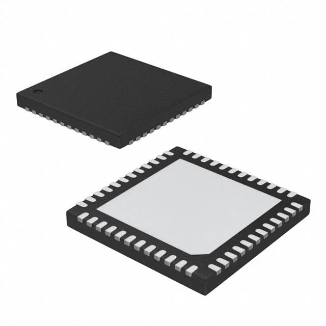
- Compact package: The A3P030-QNG48 comes in a QNG48 package, which ensures easy integration into various electronic systems.
- Reliable performance: With its robust design and high-quality components, this PLD delivers reliable and consistent performance.
Package and Quantity
The A3P030-QNG48 is packaged in a QNG48 package. Each package contains one unit of the PLD.
Specifications
- Logic elements: 30,000
- Maximum user I/Os: 48
- Operating voltage: 3.3V
- Speed grade: Standard (up to 200 MHz)
Detailed Pin Configuration
The A3P030-QNG48 has a total of 48 pins, each serving a specific function. The pin configuration is as follows:
(Pin diagram here)
Functional Features
Programmability
The A3P030-QNG48 offers extensive programmability, allowing users to define and implement complex logic functions. This flexibility enables customization and adaptation to various application requirements.
Versatile I/O Options
With 48 user I/O pins, this PLD provides ample connectivity options for interfacing with external devices and circuits. These I/O pins can be configured as inputs or outputs based on the desired functionality.
Embedded Memory
The A3P030-QNG48 includes embedded memory blocks, which can be used for storing data or implementing lookup tables. This feature enhances the device's capability to handle complex algorithms and data processing tasks.
Clock Management
This PLD incorporates dedicated clock management resources, enabling precise control over timing requirements. It supports various clocking options, including global and regional clock networks, to ensure accurate synchronization of internal logic elements.
Advantages and Disadvantages
Advantages
- High flexibility and programmability
- Low power consumption
- Compact package for easy integration
- Reliable performance
Disadvantages
- Limited logic elements compared to higher-end PLDs
- May require additional external components for certain applications
Working Principles
The A3P030-QNG48 operates based on the principles of field-programmable gate arrays (FPGAs). It consists of a matrix of configurable logic blocks interconnected through programmable routing resources. Users can program the internal connections and logic functions using hardware description languages (HDLs) or design software provided by the manufacturer.
Upon programming, the PLD configures its internal resources to implement the desired logic functions. The configured design remains persistent until reprogrammed, allowing for iterative development and testing.
Detailed Application Field Plans
The A3P030-QNG48 finds applications in various fields, including:
- Industrial Automation: Used for controlling and monitoring processes in manufacturing plants.
- Communications: Employed in networking equipment for data routing and protocol handling.
- Automotive Electronics: Integrated into automotive systems for controlling engine functions, safety features, and infotainment systems.
- Consumer Electronics: Utilized in devices such as gaming consoles, digital cameras, and home automation systems.
- Medical Devices: Incorporated into medical equipment for diagnostics, imaging, and patient monitoring.
Detailed Alternative Models
- A3P060-QNG48: Similar to the A3P030-QNG48 but with a higher logic element count (60,000).
- A3P015-QNG48: A lower-end alternative with reduced logic elements (15,000) for less complex applications.
- A3P045-QNG48: An intermediate option with increased logic elements (45,000) for more demanding designs.
These alternative models provide varying levels of performance and capacity to cater to different project requirements.
In conclusion, the A3P030-QNG48 is a versatile programmable logic device that offers high flexibility, low power consumption, and reliable performance. With its extensive application field plans and alternative models, it serves as a valuable tool in digital circuit design and implementation.
技術ソリューションにおける A3P030-QNG48 の適用に関連する 10 件の一般的な質問と回答をリストします。
Sure! Here are 10 common questions and answers related to the application of A3P030-QNG48 in technical solutions:
Q: What is A3P030-QNG48? A: A3P030-QNG48 is a specific model of programmable logic device (PLD) manufactured by Microsemi Corporation.
Q: What are the key features of A3P030-QNG48? A: Some key features of A3P030-QNG48 include 30,000 usable gates, non-volatile flash memory, low power consumption, and 48-pin QFN package.
Q: What are the typical applications of A3P030-QNG48? A: A3P030-QNG48 is commonly used in various technical solutions such as industrial automation, consumer electronics, automotive systems, and telecommunications.
Q: How can I program A3P030-QNG48? A: A3P030-QNG48 can be programmed using industry-standard hardware description languages (HDLs) like VHDL or Verilog, along with appropriate development tools provided by Microsemi.
Q: Can A3P030-QNG48 be reprogrammed after deployment? A: No, A3P030-QNG48 is a non-volatile PLD, meaning that it retains its programming even when power is removed, but it cannot be reprogrammed in the field.
Q: What is the maximum operating frequency of A3P030-QNG48? A: The maximum operating frequency of A3P030-QNG48 depends on the complexity of the design and implementation, but it can typically reach frequencies up to several hundred megahertz.
Q: Does A3P030-QNG48 support external memory interfaces? A: Yes, A3P030-QNG48 supports various external memory interfaces such as synchronous dynamic random-access memory (SDRAM), flash memory, and serial peripheral interface (SPI) flash.
Q: Can A3P030-QNG48 communicate with other devices or microcontrollers? A: Yes, A3P030-QNG48 can communicate with other devices or microcontrollers through various communication protocols like I2C, SPI, UART, or custom interfaces implemented in the design.
Q: Is A3P030-QNG48 suitable for low-power applications? A: Yes, A3P030-QNG48 is designed to be power-efficient and has low static and dynamic power consumption, making it suitable for low-power applications.
Q: Are there any development kits available for A3P030-QNG48? A: Yes, Microsemi provides development kits that include evaluation boards, software tools, documentation, and example designs to facilitate the development process using A3P030-QNG48.
Please note that the answers provided here are general and may vary depending on specific requirements and use cases.