

AT40K10-2CQC
Product Overview
Category
AT40K10-2CQC belongs to the category of programmable logic devices (PLDs).
Use
This product is primarily used in digital circuit design and implementation. It provides a flexible and customizable solution for various applications.
Characteristics
- Programmable: The AT40K10-2CQC can be programmed to perform specific functions based on the user's requirements.
- High-speed operation: It offers fast processing capabilities, making it suitable for time-critical applications.
- Versatile: The device supports a wide range of input/output configurations, allowing for diverse circuit designs.
- Low power consumption: The AT40K10-2CQC is designed to minimize power usage, making it energy-efficient.
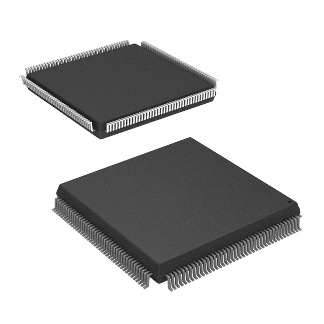
Package
The AT40K10-2CQC comes in a compact quad flat package (QFP), which ensures easy integration into circuit boards.
Essence
The essence of AT40K10-2CQC lies in its ability to provide reconfigurable logic functions, enabling users to implement complex digital circuits efficiently.
Packaging/Quantity
This product is typically packaged in reels or trays, with each containing a specified quantity of AT40K10-2CQC units. The exact packaging and quantity may vary depending on the supplier.
Specifications
- Logic elements: 10,000
- I/O pins: 32
- Operating voltage: 3.3V
- Maximum operating frequency: 100 MHz
- Programming technology: Flash-based
Detailed Pin Configuration
The AT40K10-2CQC features 32 I/O pins, each serving a specific purpose in the circuit design. The pin configuration is as follows:
- Pin 1: VCC
- Pin 2: GND
- Pin 3: I/O0
- Pin 4: I/O1
- Pin 5: I/O2
- Pin 6: I/O3
- Pin 7: I/O4
- Pin 8: I/O5
- Pin 9: I/O6
- Pin 10: I/O7
- Pin 11: I/O8
- Pin 12: I/O9
- Pin 13: I/O10
- Pin 14: I/O11
- Pin 15: I/O12
- Pin 16: I/O13
- Pin 17: I/O14
- Pin 18: I/O15
- Pin 19: I/O16
- Pin 20: I/O17
- Pin 21: I/O18
- Pin 22: I/O19
- Pin 23: I/O20
- Pin 24: I/O21
- Pin 25: I/O22
- Pin 26: I/O23
- Pin 27: I/O24
- Pin 28: I/O25
- Pin 29: I/O26
- Pin 30: I/O27
- Pin 31: I/O28
- Pin 32: I/O29
Functional Features
The AT40K10-2CQC offers several functional features that enhance its usability:
- Reconfigurability: The device can be reprogrammed multiple times, allowing for iterative design improvements and flexibility in adapting to changing requirements.
- Embedded memory: It includes on-chip memory elements that can be used to store data or configuration settings.
- Clock management: The AT40K10-2CQC supports clock signals, enabling synchronization with other components in the system.
- I/O flexibility: The device provides a wide range of input/output configurations, facilitating seamless integration with external devices.
Advantages and Disadvantages
Advantages
- Flexibility: The reconfigurable nature of AT40K10-2CQC enables rapid prototyping and design iterations.
- Cost-effective: By eliminating the need for custom hardware, this device reduces development costs.
- High performance: With its high-speed operation and large logic capacity, it can handle complex digital circuits efficiently.
Disadvantages
- Learning curve: Utilizing the full potential of AT40K10-2CQC requires familiarity with programmable logic devices and associated programming tools.
- Limited analog capabilities: As a digital device, it lacks extensive analog functionality, which may be required in certain applications.
Working Principles
The AT40K10-2CQC operates based on the principles of field-programmable gate arrays (FPGAs). It consists of configurable logic blocks (CLBs) interconnected through programmable interconnects. These CLBs contain look-up tables (LUTs), flip-flops,
技術ソリューションにおける AT40K10-2CQC の適用に関連する 10 件の一般的な質問と回答をリストします。
Sure! Here are 10 common questions and answers related to the application of AT40K10-2CQC in technical solutions:
Q: What is AT40K10-2CQC? A: AT40K10-2CQC is a specific model of Field Programmable Gate Array (FPGA) manufactured by Microchip Technology Inc.
Q: What are the key features of AT40K10-2CQC? A: Some key features of AT40K10-2CQC include 10,000 usable gates, 2,000 flip-flops, 100 MHz maximum operating frequency, and 5V power supply.
Q: How can AT40K10-2CQC be used in technical solutions? A: AT40K10-2CQC can be used for various applications such as digital signal processing, data acquisition, control systems, and communication protocols.
Q: What programming languages can be used with AT40K10-2CQC? A: AT40K10-2CQC can be programmed using Hardware Description Languages (HDLs) like VHDL or Verilog.
Q: Can AT40K10-2CQC be reprogrammed after initial configuration? A: Yes, AT40K10-2CQC is a Field Programmable device, which means it can be reprogrammed multiple times to implement different functionalities.
Q: What tools are required to program AT40K10-2CQC? A: To program AT40K10-2CQC, you will need a compatible development board, a programming cable, and software like Microchip's programming tool.
Q: What is the maximum clock frequency supported by AT40K10-2CQC? A: AT40K10-2CQC supports a maximum operating frequency of 100 MHz.
Q: Can AT40K10-2CQC interface with other components or devices? A: Yes, AT40K10-2CQC can interface with other components or devices through its I/O pins, allowing communication and data exchange.
Q: What are the power requirements for AT40K10-2CQC? A: AT40K10-2CQC operates on a 5V power supply, which should be provided within the specified voltage range.
Q: Are there any limitations or considerations when using AT40K10-2CQC? A: Some considerations include power consumption, heat dissipation, and ensuring proper signal integrity while designing the PCB layout for the application.
Please note that these answers are general and may vary depending on specific use cases and requirements.