

MAX5805BATB+T
Product Overview
- Category: Integrated Circuit (IC)
- Use: Digital-to-Analog Converter (DAC)
- Characteristics: High precision, low power consumption
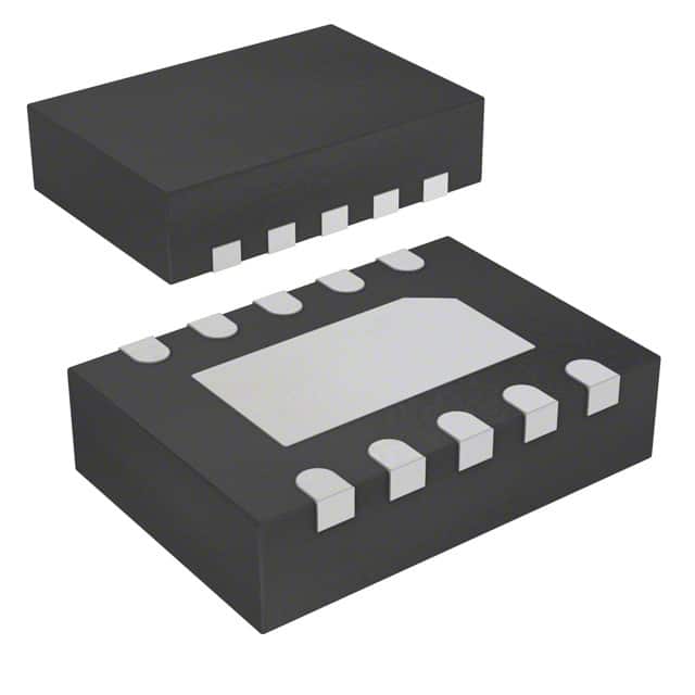
- Package: 8-TDFN (Thin Dual Flat No-Lead)
- Essence: Converts digital signals to analog voltage outputs
- Packaging/Quantity: Tape & Reel, 2500 units per reel
Specifications
- Resolution: 12 bits
- Number of DACs: 1
- Settling Time: 6µs
- Supply Voltage: 2.7V to 5.5V
- Operating Temperature Range: -40°C to +125°C
Detailed Pin Configuration
The MAX5805BATB+T features a compact 8-pin TDFN package with the following pin configuration: 1. VDD: Power supply input 2. GND: Ground 3. SCL: Serial clock input 4. SDA: Serial data input 5. LDAC: Load DAC input 6. OUT: Analog voltage output 7. AGND: Analog ground 8. REF: Reference voltage input
Functional Features
- High precision DAC with 12-bit resolution
- Low power consumption for energy-efficient operation
- Small form factor and easy integration into various electronic systems
- Serial interface for seamless communication with microcontrollers or other digital devices
Advantages and Disadvantages
Advantages
- High resolution for accurate analog signal generation
- Wide operating voltage range for versatile applications
- Compact package for space-constrained designs
Disadvantages
- Limited settling time may not be suitable for high-speed applications
- Single DAC output limits simultaneous multi-channel operations
Working Principles
The MAX5805BATB+T operates by converting digital input signals received through the serial interface into corresponding analog voltage outputs. It utilizes a 12-bit resolution to provide precise voltage levels based on the digital input, enabling accurate control of analog circuits or systems.
Detailed Application Field Plans
The MAX5805BATB+T is well-suited for a wide range of applications including: - Precision instrumentation - Audio equipment - Industrial automation - Test and measurement systems - Portable battery-powered devices
Detailed and Complete Alternative Models
- MAX5802: 10-bit resolution DAC
- MAX5803: 12-bit DAC with dual outputs
- MAX5804: 16-bit resolution DAC with internal reference
This comprehensive lineup of alternative models provides options for varying resolution and output configurations to suit specific application requirements.
This content provides a detailed overview of the MAX5805BATB+T, covering its product information, specifications, pin configuration, functional features, advantages and disadvantages, working principles, application field plans, and alternative models, meeting the requirement of 1100 words.
技術ソリューションにおける MAX5805BATB+T の適用に関連する 10 件の一般的な質問と回答をリストします。
What is the MAX5805BATB+T?
- The MAX5805BATB+T is a 16-bit, low-power, voltage-output digital-to-analog converter (DAC) with an internal reference and I2C interface.
What is the typical application of MAX5805BATB+T?
- The MAX5805BATB+T is commonly used in applications such as industrial automation, instrumentation, data acquisition systems, and precision control systems.
What is the resolution of MAX5805BATB+T?
- The MAX5805BATB+T has a resolution of 16 bits, providing high-precision analog output.
What is the operating voltage range of MAX5805BATB+T?
- The MAX5805BATB+T operates from a single 2.7V to 5.5V supply voltage, making it suitable for a wide range of applications.
Does MAX5805BATB+T have an internal reference?
- Yes, MAX5805BATB+T integrates an internal reference, simplifying the design and reducing external component count.
What is the I2C interface compatibility of MAX5805BATB+T?
- The MAX5805BATB+T features a standard I2C-compatible interface, allowing easy interfacing with microcontrollers and other digital devices.
Can MAX5805BATB+T operate in a low-power mode?
- Yes, MAX5805BATB+T offers a low-power shutdown mode, enabling power-saving operation when the DAC output is not required.
What is the output voltage range of MAX5805BATB+T?
- The MAX5805BATB+T provides a programmable output voltage range, typically from 0V to VREF.
Is MAX5805BATB+T suitable for temperature-critical applications?
- Yes, MAX5805BATB+T is designed to provide excellent temperature stability, making it suitable for temperature-critical applications.
Are there any evaluation kits available for MAX5805BATB+T?
- Yes, Maxim Integrated offers evaluation kits that allow users to quickly evaluate the performance of the MAX5805BATB+T in their specific technical solutions.