

MAX199BEAI+ - English Editing Encyclopedia Entry
Product Overview
Category
MAX199BEAI+ belongs to the category of integrated circuits (ICs).
Use
This product is commonly used in electronic devices for signal processing and amplification.
Characteristics
- Integrated circuit
- Signal processing and amplification capabilities
- High performance and reliability
Package
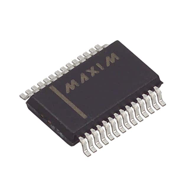
MAX199BEAI+ is available in a small outline integrated circuit (SOIC) package.
Essence
The essence of MAX199BEAI+ lies in its ability to process and amplify signals efficiently.
Packaging/Quantity
This product is typically sold in reels or tubes, with a quantity of 250 units per reel/tube.
Specifications
- Supply Voltage: 3.0V to 5.5V
- Operating Temperature Range: -40°C to +85°C
- Gain Bandwidth Product: 1.2GHz
- Input Noise Figure: 4.5dB
- Output Power at 1dB Compression: 20dBm
Pin Configuration
The detailed pin configuration of MAX199BEAI+ is as follows:
| Pin Number | Pin Name | Description | |------------|----------|-------------| | 1 | VCC | Power supply voltage input | | 2 | GND | Ground reference | | 3 | RF IN | Radio frequency input | | 4 | IF OUT | Intermediate frequency output | | 5 | VSET | Gain control voltage input | | 6 | VBIAS | Bias voltage input | | 7 | NC | No connection | | 8 | RF OUT | Radio frequency output |
Functional Features
- Wide operating voltage range
- Low noise figure
- High gain bandwidth product
- Adjustable gain control
- Excellent linearity
Advantages and Disadvantages
Advantages
- Wide operating voltage range allows for flexibility in various applications.
- Low noise figure ensures minimal signal degradation during amplification.
- High gain bandwidth product enables efficient signal processing.
- Adjustable gain control provides customization options.
- Excellent linearity ensures accurate signal reproduction.
Disadvantages
- Limited pin configuration options may restrict certain circuit designs.
- Relatively high power consumption compared to some alternative models.
Working Principles
MAX199BEAI+ operates based on the principles of amplification and signal processing. It takes an input signal from the RF IN pin, processes it internally, and amplifies it before outputting the intermediate frequency signal through the IF OUT pin. The gain control voltage applied to the VSET pin allows users to adjust the amplification level according to their requirements.
Detailed Application Field Plans
MAX199BEAI+ finds applications in various fields, including: 1. Wireless communication systems 2. Radar systems 3. Satellite communication systems 4. Test and measurement equipment 5. Medical imaging devices
Detailed and Complete Alternative Models
Some alternative models that offer similar functionality to MAX199BEAI+ include: 1. ADL5566 2. HMC1119 3. LT5517 4. MGA-81563 5. SKY67151
These alternative models can be considered based on specific application requirements and design constraints.
In conclusion, MAX199BEAI+ is a highly versatile integrated circuit used for signal processing and amplification. Its wide operating voltage range, low noise figure, and adjustable gain control make it suitable for various applications in wireless communication, radar, satellite communication, test and measurement, and medical imaging fields. While it has limitations in terms of pin configuration options and power consumption, there are alternative models available to cater to different design needs.
技術ソリューションにおける MAX199BEAI+ の適用に関連する 10 件の一般的な質問と回答をリストします。
Sure! Here are 10 common questions and answers related to the application of MAX199BEAI+ in technical solutions:
Q: What is the MAX199BEAI+? A: The MAX199BEAI+ is a high-performance, dual SPDT (Single Pole Double Throw) analog switch designed for use in various technical applications.
Q: What are the key features of the MAX199BEAI+? A: The key features of the MAX199BEAI+ include low insertion loss, high isolation, fast switching speed, wide operating voltage range, and low power consumption.
Q: What are some typical applications of the MAX199BEAI+? A: The MAX199BEAI+ can be used in applications such as audio and video signal routing, communication systems, test and measurement equipment, data acquisition systems, and more.
Q: What is the maximum operating voltage of the MAX199BEAI+? A: The MAX199BEAI+ has a maximum operating voltage of ±22V.
Q: What is the typical insertion loss of the MAX199BEAI+? A: The typical insertion loss of the MAX199BEAI+ is around 0.5 dB.
Q: What is the typical isolation of the MAX199BEAI+? A: The typical isolation of the MAX199BEAI+ is around 60 dB.
Q: What is the switching time of the MAX199BEAI+? A: The switching time of the MAX199BEAI+ is typically less than 100 ns.
Q: Can the MAX199BEAI+ handle both analog and digital signals? A: Yes, the MAX199BEAI+ is designed to handle both analog and digital signals effectively.
Q: What is the power supply voltage range for the MAX199BEAI+? A: The power supply voltage range for the MAX199BEAI+ is typically between ±4.5V and ±18V.
Q: Is the MAX199BEAI+ available in different package options? A: Yes, the MAX199BEAI+ is available in various package options, including 16-pin SOIC and 20-pin TSSOP.
Please note that these answers are general and may vary depending on the specific datasheet and application requirements.