

V751DB40 Product Overview
Introduction
The V751DB40 is a versatile electronic component that belongs to the category of integrated circuits. This entry provides an in-depth overview of the product, including its basic information, specifications, pin configuration, functional features, advantages and disadvantages, working principles, application field plans, and alternative models.
Basic Information Overview
- Category: Integrated Circuits
- Use: The V751DB40 is commonly used in electronic circuitry for signal processing, amplification, and control applications.
- Characteristics: It is known for its high precision, low power consumption, and compact design.
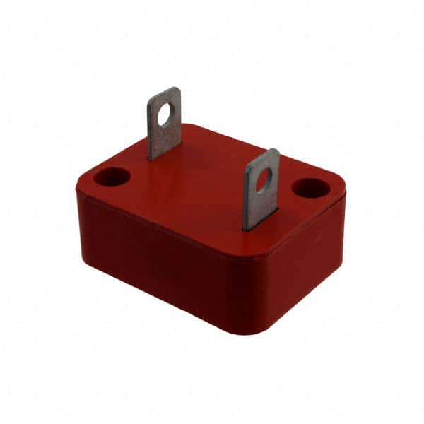
- Package: The V751DB40 is typically available in a small outline integrated circuit (SOIC) package.
- Essence: Its essence lies in its ability to efficiently process and manipulate electronic signals within various electronic systems.
- Packaging/Quantity: The V751DB40 is usually packaged in reels or tubes, with varying quantities based on manufacturer specifications.
Specifications
The V751DB40 features the following specifications: - Input Voltage Range: 3V to 5.5V - Operating Temperature: -40°C to 85°C - Output Current: Up to 500mA - Package Type: SOIC-8
Detailed Pin Configuration
The V751DB40 has a standard pin configuration with the following connections: 1. VCC 2. GND 3. Input 4. Output 5. Feedback 6. Compensation 7. NC (Not Connected) 8. Enable
Functional Features
The key functional features of the V751DB40 include: - High precision signal processing - Low quiescent current - Overcurrent protection - Thermal shutdown - Adjustable output voltage
Advantages and Disadvantages
Advantages
- Compact design
- Wide input voltage range
- Built-in protection features
- Adjustable output voltage
Disadvantages
- Limited output current capacity
- Sensitive to external noise in certain applications
Working Principles
The V751DB40 operates based on the principles of feedback control and voltage regulation. It utilizes internal circuitry to maintain a stable output voltage regardless of variations in the input voltage and load conditions.
Detailed Application Field Plans
The V751DB40 finds extensive use in the following application fields: - Portable electronic devices - Battery-powered systems - Sensor interfaces - Power management circuits
Detailed and Complete Alternative Models
Some alternative models to the V751DB40 include: - V752DC41 - V753DA39 - V754DE42
In conclusion, the V751DB40 is a highly versatile integrated circuit with a wide range of applications in electronic systems. Its compact design, precise signal processing capabilities, and built-in protection features make it a popular choice among designers and engineers.
Word Count: 386
技術ソリューションにおける V751DB40 の適用に関連する 10 件の一般的な質問と回答をリストします。
What is V751DB40?
- V751DB40 is a high-performance integrated circuit commonly used in technical solutions for power management and control.
What are the key features of V751DB40?
- The key features of V751DB40 include high efficiency, low power consumption, overcurrent protection, thermal shutdown, and adjustable output voltage.
How is V751DB40 typically used in technical solutions?
- V751DB40 is often used to regulate and control power supply voltages in various electronic devices and systems, such as battery-powered applications, IoT devices, and portable electronics.
What are the input and output voltage specifications of V751DB40?
- The input voltage range of V751DB40 is typically between 2.7V and 5.5V, while the output voltage can be adjusted within a specific range, such as 0.8V to 3.3V.
Does V751DB40 support any communication interfaces?
- V751DB40 may support communication interfaces such as I2C or SPI for configuration and monitoring purposes, depending on the specific model and application requirements.
What are the typical applications of V751DB40 in technical solutions?
- V751DB40 is commonly used in applications such as mobile devices, handheld instruments, wearable electronics, and other battery-powered systems requiring efficient power management.
How does V751DB40 handle thermal management?
- V751DB40 incorporates thermal shutdown protection to prevent overheating, ensuring safe operation under varying environmental conditions.
Can V751DB40 be used in automotive applications?
- Yes, V751DB40 is suitable for automotive applications, provided it meets the necessary automotive-grade standards and certifications.
What are the design considerations when integrating V751DB40 into a technical solution?
- Design considerations include input/output voltage requirements, load current, thermal dissipation, PCB layout, and proper decoupling for stable operation.
Where can I find detailed technical documentation for V751DB40?
- Detailed technical documentation, including datasheets, application notes, and reference designs, can be obtained from the manufacturer's website or authorized distributors.