

P6SMB8.2A - Product Overview and Analysis
Introduction
The P6SMB8.2A is a crucial component in the field of electronics, specifically within the category of transient voltage suppressor (TVS) diodes. This entry will provide an in-depth overview of the P6SMB8.2A, covering its basic information, specifications, pin configuration, functional features, advantages and disadvantages, working principles, application field plans, and alternative models.
Basic Information Overview
- Category: Transient Voltage Suppressor (TVS) Diode
- Use: Protection against voltage transients in electronic circuits
- Characteristics: Fast response time, low clamping voltage, high surge current capability
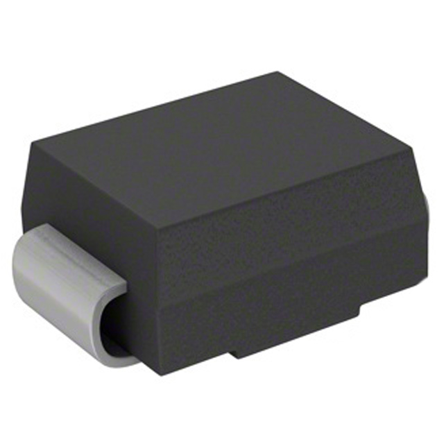
- Package: SMB (DO-214AA)
- Essence: Safeguarding sensitive electronic components from voltage spikes
- Packaging/Quantity: Typically available in reels or tubes, quantity varies by manufacturer
Specifications
- Voltage - Reverse Standoff (Typ): 7.37V
- Voltage - Breakdown (Min): 8.22V
- Voltage - Clamping (Max) @ Ipp: 14.5V
- Current - Peak Pulse (10/1000µs): 53.3A
- Power - Peak Pulse: 600W
- Type: Zener
- Mounting Type: Surface Mount
- Package / Case: DO-214AA, SMB
- Operating Temperature: -55°C ~ 150°C
Detailed Pin Configuration
The P6SMB8.2A typically follows the standard pin configuration for SMB diodes, with two leads for surface mounting onto circuit boards.
Functional Features
- Transient Voltage Suppression: Rapidly clamps transient voltages to protect downstream components.
- Fast Response Time: Reacts quickly to voltage spikes, minimizing potential damage.
- High Surge Current Capability: Can handle substantial surge currents without failing.
Advantages and Disadvantages
Advantages
- Effective protection against voltage transients
- Fast response time
- Compact surface mount package
Disadvantages
- Limited power dissipation capability compared to larger TVS diodes
- May require additional circuitry for comprehensive overvoltage protection
Working Principles
The P6SMB8.2A operates based on the principle of zener breakdown, where it rapidly conducts when the voltage across it exceeds the breakdown voltage, diverting excess current away from sensitive components.
Detailed Application Field Plans
The P6SMB8.2A finds extensive use in various applications, including: - Telecommunications: Protecting communication equipment from lightning-induced surges - Consumer Electronics: Safeguarding sensitive circuits in devices like smartphones and tablets - Automotive Electronics: Shielding vehicle electronics from voltage spikes
Detailed and Complete Alternative Models
- P6SMB6.8A: Lower breakdown voltage variant
- P6SMB10A: Higher breakdown voltage variant
- 1.5SMC8.2A: Alternative package (1.5SMC) with similar characteristics
In conclusion, the P6SMB8.2A plays a vital role in protecting electronic circuits from voltage transients, offering fast response times and high surge current capabilities. While it has limitations in power dissipation, its compact size and effectiveness make it a popular choice in various industries.
Word Count: 498
技術ソリューションにおける P6SMB8.2A の適用に関連する 10 件の一般的な質問と回答をリストします。
What is the maximum peak pulse power of P6SMB8.2A?
- The maximum peak pulse power of P6SMB8.2A is 600 watts.
What is the breakdown voltage of P6SMB8.2A?
- The breakdown voltage of P6SMB8.2A is 7.37V to 8.23V.
What is the typical clamping voltage of P6SMB8.2A?
- The typical clamping voltage of P6SMB8.2A is 11.4V at 10A.
What is the operating temperature range for P6SMB8.2A?
- The operating temperature range for P6SMB8.2A is -55°C to +150°C.
What are the applications of P6SMB8.2A in technical solutions?
- P6SMB8.2A is commonly used for transient voltage suppression in various electronic systems, including telecommunications equipment, industrial control systems, and automotive electronics.
What is the reverse stand-off voltage of P6SMB8.2A?
- The reverse stand-off voltage of P6SMB8.2A is 7.37V.
Is P6SMB8.2A RoHS compliant?
- Yes, P6SMB8.2A is RoHS compliant, making it suitable for use in environmentally conscious designs.
What is the package type of P6SMB8.2A?
- P6SMB8.2A is available in a DO-214AA (SMB) package.
What are the key features of P6SMB8.2A?
- Key features of P6SMB8.2A include low incremental surge resistance, fast response time, and high reliability.
What are the recommended storage conditions for P6SMB8.2A?
- It is recommended to store P6SMB8.2A in a dry environment with a temperature range of -55°C to +150°C to maintain its performance and reliability.