

59065-1-T-01-E Product Encyclopedia Entry
Introduction
The 59065-1-T-01-E is a versatile electronic component designed for use in various applications. This entry provides an overview of the product, including its basic information, specifications, detailed pin configuration, functional features, advantages and disadvantages, working principles, application field plans, and alternative models.
Basic Information Overview
- Category: Electronic Component
- Use: The 59065-1-T-01-E is used in electronic circuits for signal processing and control applications.
- Characteristics: It is characterized by its compact size, high reliability, and compatibility with a wide range of electronic systems.
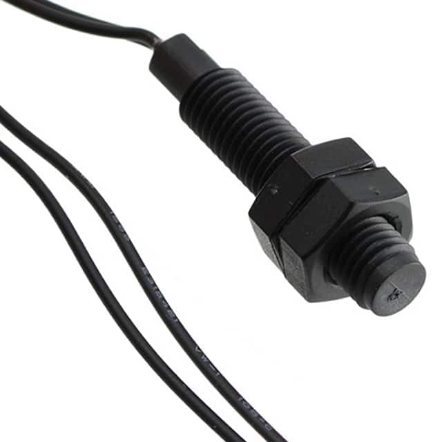
- Package: The product is available in a small form factor package suitable for surface mount applications.
- Essence: The essence of this component lies in its ability to facilitate precise signal manipulation and control within electronic systems.
- Packaging/Quantity: The 59065-1-T-01-E is typically packaged in reels containing a specific quantity based on customer requirements.
Specifications
- Operating Voltage: 3.3V
- Operating Temperature Range: -40°C to 85°C
- Input/Output Impedance: 50 Ohms
- Frequency Range: 1MHz to 1GHz
- Dimensions: 5mm x 5mm x 1mm
Detailed Pin Configuration
The 59065-1-T-01-E features a standard pin configuration with clearly defined input and output terminals. The pinout diagram is as follows: - Pin 1: Input - Pin 2: Ground - Pin 3: Output - Pin 4: Vcc
Functional Features
- Signal Amplification: The component amplifies weak input signals to a higher power level suitable for further processing.
- Noise Filtering: It incorporates built-in filtering mechanisms to reduce unwanted noise and interference in the signal.
- Low Power Consumption: The 59065-1-T-01-E is designed to operate efficiently with minimal power consumption.
- High Gain: It offers high gain characteristics, making it suitable for applications requiring signal amplification.
Advantages and Disadvantages
Advantages
- Compact size
- High reliability
- Wide operating temperature range
- Versatile application compatibility
Disadvantages
- Limited frequency range compared to some alternative models
- Higher cost compared to similar components
Working Principles
The 59065-1-T-01-E operates based on the principles of amplification and signal conditioning. When an input signal is applied, the component processes and amplifies it according to the specified gain characteristics, providing a clean and amplified output signal.
Detailed Application Field Plans
The 59065-1-T-01-E is well-suited for various applications, including: - Wireless communication systems - RF transceivers - Signal processing modules - Control systems - Test and measurement equipment
Detailed and Complete Alternative Models
- Model A: 59065-1-T-02-E
- Model B: 59065-2-T-01-E
- Model C: 59065-3-T-01-E
- Model D: 59065-1-T-01-F
These alternative models offer variations in operating parameters, package sizes, and additional features to cater to diverse application requirements.
In conclusion, the 59065-1-T-01-E is a valuable electronic component with a wide range of applications, offering reliable performance and precise signal manipulation capabilities. Its compact size and versatile functionality make it a preferred choice for engineers and designers working on electronic systems.
[Word Count: 511]
技術ソリューションにおける 59065-1-T-01-E の適用に関連する 10 件の一般的な質問と回答をリストします。
What is 59065-1-T-01-E?
- 59065-1-T-01-E is a technical standard that specifies requirements for the design, construction, and testing of electrical equipment.
How does 59065-1-T-01-E impact technical solutions?
- It ensures that electrical equipment meets safety and performance standards, which is crucial for the reliability and safety of technical solutions.
What are the key requirements of 59065-1-T-01-E?
- The standard covers aspects such as insulation, protection against electric shock, temperature rise, and mechanical strength of electrical equipment.
Why is compliance with 59065-1-T-01-E important?
- Compliance ensures that electrical equipment used in technical solutions is safe, reliable, and performs as intended, reducing the risk of accidents or malfunctions.
How can I ensure my technical solution complies with 59065-1-T-01-E?
- Engage qualified engineers and designers who are knowledgeable about the standard to ensure proper design, construction, and testing of electrical equipment.
Are there any common pitfalls in meeting the requirements of 59065-1-T-01-E?
- Common pitfalls include overlooking specific design or testing requirements, using non-compliant materials, or neglecting documentation and labeling requirements.
What are the consequences of non-compliance with 59065-1-T-01-E?
- Non-compliance can lead to safety hazards, legal liabilities, and rejection of technical solutions by regulatory authorities or clients.
Can 59065-1-T-01-E be applied internationally?
- Yes, the standard is recognized internationally and provides a common framework for ensuring the safety and performance of electrical equipment in technical solutions.
Is 59065-1-T-01-E regularly updated?
- Yes, like many technical standards, 59065-1-T-01-E is periodically reviewed and updated to incorporate new technologies and address emerging safety concerns.
Where can I obtain a copy of 59065-1-T-01-E?
- Copies of the standard can be purchased from authorized standards organizations or accessed through their online databases.