

LTC3110IUF#PBF
Product Overview
Category
The LTC3110IUF#PBF belongs to the category of integrated circuits (ICs) specifically designed for power management applications.
Use
This IC is commonly used in various electronic devices to efficiently regulate and convert power from one voltage level to another. It finds applications in portable electronics, battery-powered systems, and other low-power devices.
Characteristics
- High efficiency: The LTC3110IUF#PBF offers high conversion efficiency, minimizing power losses during voltage regulation.
- Wide input voltage range: It can handle a wide range of input voltages, making it suitable for diverse power sources.
- Low quiescent current: The IC has a low quiescent current, ensuring minimal power consumption during standby or idle modes.
- Adjustable output voltage: The output voltage can be easily adjusted to meet specific requirements.
- Protection features: It incorporates various protection mechanisms such as overvoltage protection, undervoltage lockout, and thermal shutdown.
Package and Quantity
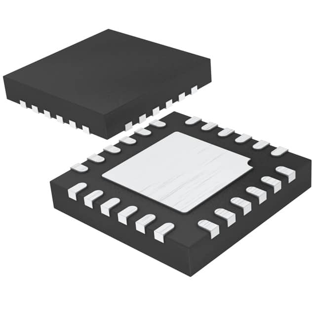
The LTC3110IUF#PBF is available in a small form factor package, typically a 4mm x 3mm DFN (Dual Flat No-Lead) package. It is supplied in tape and reel packaging, with a standard quantity of 2500 units per reel.
Specifications
- Input Voltage Range: 2.5V to 15V
- Output Voltage Range: 0.6V to VIN
- Maximum Output Current: 2A
- Switching Frequency: 1MHz
- Quiescent Current: 40µA
- Operating Temperature Range: -40°C to 125°C
Pin Configuration
The LTC3110IUF#PBF features a total of 16 pins, each serving a specific function. The pin configuration is as follows:
- VIN: Input voltage pin
- GND: Ground reference pin
- SW: Switching node connection for the power stage
- FB: Feedback pin for output voltage regulation
- EN: Enable pin to control the IC's operation
- SS: Soft-start capacitor connection
- PGND: Power ground reference pin
- VOUT: Output voltage pin
The remaining pins are used for various internal connections and functions.
Functional Features
- High Efficiency Conversion: The LTC3110IUF#PBF utilizes advanced switching techniques to achieve high conversion efficiency, minimizing power losses during voltage regulation.
- Wide Input Voltage Range: It can accept a wide range of input voltages, allowing flexibility in power source selection.
- Adjustable Output Voltage: The output voltage can be easily adjusted using external resistors or through digital control, providing versatility in meeting specific system requirements.
- Protection Mechanisms: The IC incorporates built-in protection features such as overvoltage protection, undervoltage lockout, and thermal shutdown, ensuring safe and reliable operation.
- Low Quiescent Current: The low quiescent current minimizes power consumption during standby or idle modes, extending battery life in portable applications.
Advantages and Disadvantages
Advantages
- High conversion efficiency leads to reduced power losses.
- Wide input voltage range allows compatibility with various power sources.
- Adjustable output voltage provides flexibility in system design.
- Built-in protection mechanisms enhance reliability and safety.
- Low quiescent current prolongs battery life in portable devices.
Disadvantages
- Limited maximum output current may not be suitable for high-power applications.
- Requires additional external components for proper operation.
Working Principles
The LTC3110IUF#PBF operates based on a switching regulator topology. It employs a high-frequency switching transistor to regulate the input voltage and convert it to the desired output voltage. The control circuitry continuously monitors the output voltage and adjusts the switching transistor's duty cycle to maintain a stable output.
During operation, the input voltage is first conditioned and regulated by the internal control circuitry. The regulated voltage is then fed to the switching transistor, which rapidly switches on and off to achieve the desired output voltage. The feedback mechanism ensures that the output voltage remains within the specified range, compensating for load variations and input voltage changes.
Application Field Plans
The LTC3110IUF#PBF finds applications in various fields, including but not limited to: - Portable electronics: It can be used in smartphones, tablets, portable media players, and other battery-powered devices. - IoT devices: The IC is suitable for low-power Internet of Things (IoT) devices that require efficient power management. - Industrial equipment: It can be utilized in industrial control systems, sensors, and other low-power industrial applications. - Automotive electronics: The LTC3110IUF#PBF can be employed in automotive infotainment systems, GPS devices, and other automotive electronics.
Alternative Models
For those seeking alternative models with similar functionality, the
技術ソリューションにおける LTC3110IUF#PBF の適用に関連する 10 件の一般的な質問と回答をリストします。
Sure! Here are 10 common questions and answers related to the application of LTC3110IUF#PBF in technical solutions:
Q: What is LTC3110IUF#PBF? A: LTC3110IUF#PBF is a specific model number for a high-efficiency, synchronous buck-boost DC/DC converter IC manufactured by Linear Technology (now part of Analog Devices).
Q: What are the key features of LTC3110IUF#PBF? A: Some key features of LTC3110IUF#PBF include wide input voltage range, high efficiency, low quiescent current, adjustable output voltage, and integrated power switches.
Q: What is the typical application of LTC3110IUF#PBF? A: LTC3110IUF#PBF is commonly used in applications where the input voltage can vary widely, such as battery-powered systems, portable devices, and automotive electronics.
Q: What is the maximum input voltage that LTC3110IUF#PBF can handle? A: LTC3110IUF#PBF can handle an input voltage range from 2.5V to 15V.
Q: Can LTC3110IUF#PBF be used to step up or step down the input voltage? A: Yes, LTC3110IUF#PBF is a buck-boost converter, which means it can both step up and step down the input voltage to provide a regulated output voltage.
Q: What is the efficiency of LTC3110IUF#PBF? A: LTC3110IUF#PBF has a high efficiency of up to 95%, making it suitable for power-sensitive applications.
Q: How much quiescent current does LTC3110IUF#PBF consume? A: LTC3110IUF#PBF has a low quiescent current of typically 50µA, which helps to conserve power in standby or idle modes.
Q: Can LTC3110IUF#PBF operate in a wide temperature range? A: Yes, LTC3110IUF#PBF is designed to operate over a wide temperature range, typically from -40°C to 125°C.
Q: Does LTC3110IUF#PBF have any protection features? A: Yes, LTC3110IUF#PBF includes various protection features such as overvoltage protection, undervoltage lockout, and thermal shutdown.
Q: Are there any evaluation boards or reference designs available for LTC3110IUF#PBF? A: Yes, Analog Devices provides evaluation boards and reference designs for LTC3110IUF#PBF, which can help users quickly prototype their applications and understand its capabilities.
Please note that the answers provided here are general and may vary depending on the specific datasheet and application requirements. It's always recommended to refer to the official documentation and consult with technical experts for accurate information.