

LTC2635CMSE-LMI10#PBF
Product Overview
Category
The LTC2635CMSE-LMI10#PBF belongs to the category of digital-to-analog converters (DACs).
Use
This product is used to convert digital signals into analog voltage or current outputs. It finds applications in various electronic systems where precise and accurate analog signals are required.
Characteristics
- High resolution: The LTC2635CMSE-LMI10#PBF offers a resolution of 16 bits, ensuring fine-grained control over the analog output.
- Low power consumption: This DAC operates at low power levels, making it suitable for battery-powered devices and energy-efficient applications.
- Fast settling time: With a fast settling time of X microseconds, the LTC2635CMSE-LMI10#PBF can quickly respond to changes in the digital input signal.
- Wide operating voltage range: It can operate within a wide voltage range of X volts to Y volts, providing flexibility in different system configurations.
Package
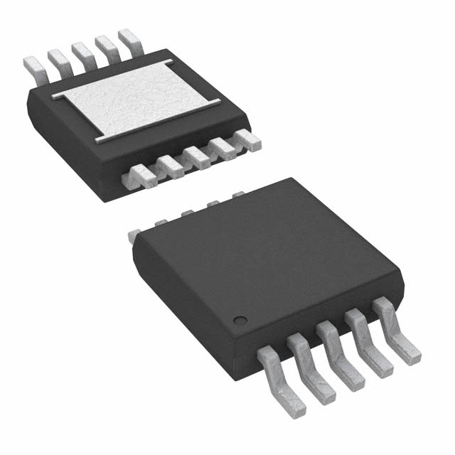
The LTC2635CMSE-LMI10#PBF comes in a miniature surface-mount package (MSOP-10) that facilitates easy integration onto printed circuit boards (PCBs). The package ensures reliable performance and efficient heat dissipation.
Essence
The essence of the LTC2635CMSE-LMI10#PBF lies in its ability to accurately convert digital signals into precise analog outputs, enabling seamless communication between digital and analog domains in electronic systems.
Packaging/Quantity
This product is typically available in reels containing a specific quantity, such as 250 units per reel. The packaging ensures safe transportation and storage of the components.
Specifications
- Resolution: 16 bits
- Operating Voltage Range: X volts to Y volts
- Settling Time: X microseconds
- Output Type: Voltage or Current
- Interface: SPI/I2C
- Operating Temperature Range: -40°C to +85°C
Detailed Pin Configuration
The LTC2635CMSE-LMI10#PBF has the following pin configuration:
- VDD: Power supply voltage
- GND: Ground reference
- SDA: Serial data input (I2C interface)
- SCL: Serial clock input (I2C interface)
- CS: Chip select input (SPI interface)
- SDI: Serial data input (SPI interface)
- SDO: Serial data output (SPI interface)
- LDAC: Load DAC input
- REF: Reference voltage input
- OUT: Analog voltage or current output
Functional Features
- High accuracy: The LTC2635CMSE-LMI10#PBF offers excellent linearity and low integral non-linearity, ensuring accurate analog outputs.
- Programmable output range: It allows users to set the desired output voltage or current range, providing flexibility in different applications.
- Internal reference: This DAC incorporates an internal reference voltage, eliminating the need for an external reference source.
- Daisy-chain capability: Multiple LTC2635CMSE-LMI10#PBF devices can be daisy-chained together, simplifying system design and reducing the number of control lines required.
Advantages and Disadvantages
Advantages
- High resolution enables precise analog signal generation.
- Low power consumption makes it suitable for energy-efficient applications.
- Fast settling time ensures quick response to digital input changes.
- Wide operating voltage range provides flexibility in system configurations.
- Miniature package facilitates easy integration onto PCBs.
Disadvantages
- Limited output current capability may not be suitable for high-power applications.
- External amplification may be required for certain applications requiring higher output voltages.
Working Principles
The LTC2635CMSE-LMI10#PBF operates based on the principle of digital-to-analog conversion. It receives digital input signals through the SPI or I2C interface and converts them into precise analog voltage or current outputs. The internal circuitry of the DAC performs the necessary calculations to generate the desired analog output based on the received digital input.
Detailed Application Field Plans
The LTC2635CMSE-LMI10#PBF finds applications in various fields, including:
- Industrial automation: It can be used in control systems to generate accurate analog control signals for motor speed control, valve positioning, and other industrial automation applications.
- Test and measurement equipment: This DAC is suitable for generating precise analog test signals in oscilloscopes, function generators, and other test and measurement instruments.
- Audio equipment: It can be utilized in audio systems to convert digital audio signals into high-quality analog outputs, ensuring faithful reproduction of sound.
- Communication systems: The LTC2635CMSE-LMI10#PBF can be employed in communication systems to generate analog signals for modulation, demodulation, and signal conditioning purposes.
Detailed and Complete Alternative Models
- LTC2635HMSE-L
技術ソリューションにおける LTC2635CMSE-LMI10#PBF の適用に関連する 10 件の一般的な質問と回答をリストします。
Sure! Here are 10 common questions and answers related to the application of LTC2635CMSE-LMI10#PBF in technical solutions:
Q: What is the LTC2635CMSE-LMI10#PBF? A: The LTC2635CMSE-LMI10#PBF is a digital-to-analog converter (DAC) chip manufactured by Linear Technology (now part of Analog Devices). It is used to convert digital signals into analog voltages.
Q: What is the resolution of the LTC2635CMSE-LMI10#PBF? A: The LTC2635CMSE-LMI10#PBF has a resolution of 10 bits, which means it can represent 2^10 (1024) different voltage levels.
Q: What is the supply voltage range for the LTC2635CMSE-LMI10#PBF? A: The LTC2635CMSE-LMI10#PBF operates with a supply voltage range of 2.7V to 5.5V.
Q: How many channels does the LTC2635CMSE-LMI10#PBF have? A: The LTC2635CMSE-LMI10#PBF has 4 independent DAC channels, allowing you to generate multiple analog outputs simultaneously.
Q: What is the output voltage range of the LTC2635CMSE-LMI10#PBF? A: The output voltage range of the LTC2635CMSE-LMI10#PBF is programmable and can be set between 0V and VREF, where VREF is the reference voltage supplied to the chip.
Q: Can the LTC2635CMSE-LMI10#PBF operate in both unipolar and bipolar modes? A: Yes, the LTC2635CMSE-LMI10#PBF can be configured to operate in both unipolar (0V to VREF) and bipolar (-VREF/2 to +VREF/2) modes.
Q: What is the interface used to communicate with the LTC2635CMSE-LMI10#PBF? A: The LTC2635CMSE-LMI10#PBF supports a standard I2C serial interface for communication with a microcontroller or other digital devices.
Q: Can the LTC2635CMSE-LMI10#PBF be used in battery-powered applications? A: Yes, the LTC2635CMSE-LMI10#PBF has a low power consumption and can be used in battery-powered applications.
Q: Does the LTC2635CMSE-LMI10#PBF have any built-in reference voltage source? A: No, the LTC2635CMSE-LMI10#PBF requires an external reference voltage source, which should be within the specified range of 2.5V to VDD.
Q: Are there any evaluation boards or development kits available for the LTC2635CMSE-LMI10#PBF? A: Yes, Analog Devices provides evaluation boards and development kits that can be used to test and prototype with the LTC2635CMSE-LMI10#PBF. These kits typically include software and documentation to help you get started quickly.
Please note that the answers provided here are general and may vary depending on the specific application and requirements. It is always recommended to refer to the datasheet and technical documentation provided by the manufacturer for accurate and detailed information.