

LTC2624CGN-1#PBF
Product Overview
Category
The LTC2624CGN-1#PBF belongs to the category of digital-to-analog converters (DACs).
Use
This product is used to convert digital signals into analog voltage or current outputs.
Characteristics
- High precision and accuracy
- Low power consumption
- Wide operating temperature range
- Small package size
- Easy integration with microcontrollers and other digital systems
Package
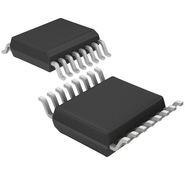
The LTC2624CGN-1#PBF is available in a 16-pin SSOP (Shrink Small Outline Package) package.
Essence
The essence of the LTC2624CGN-1#PBF is its ability to provide accurate analog outputs based on digital input signals.
Packaging/Quantity
This product is typically packaged in reels or tubes, with a quantity of 250 units per reel/tube.
Specifications
- Resolution: 12 bits
- Number of Channels: 4
- Output Type: Voltage
- Supply Voltage Range: 2.7V to 5.5V
- Operating Temperature Range: -40°C to +85°C
- Interface: SPI (Serial Peripheral Interface)
- DNL (Differential Non-Linearity): ±0.5 LSB (Least Significant Bit)
- INL (Integral Non-Linearity): ±1 LSB
Detailed Pin Configuration
The LTC2624CGN-1#PBF has a total of 16 pins, which are assigned specific functions as follows:
- VDD: Power supply voltage
- GND: Ground reference
- CS: Chip select input for SPI communication
- SCK: Serial clock input for SPI communication
- SDI: Serial data input for SPI communication
- LDAC: Load DAC input for simultaneous update of all channels
- REF: Reference voltage input
- OUTA: Analog output for Channel A
- OUTB: Analog output for Channel B
- OUTC: Analog output for Channel C
- OUTD: Analog output for Channel D 12-16. NC: No connection
Functional Features
- Simultaneous update of all channels
- Low glitch energy
- Power-on reset to zero-scale or mid-scale output voltage
- Internal reference voltage (2.048V)
- Software programmable output range and power-down mode
- Daisy-chainable SPI interface for multiple devices
Advantages and Disadvantages
Advantages
- High precision and accuracy in analog output
- Low power consumption, suitable for battery-powered applications
- Wide operating temperature range allows usage in various environments
- Small package size enables space-constrained designs
- Easy integration with microcontrollers and digital systems
Disadvantages
- Limited number of channels (4)
- Requires external reference voltage for accurate operation
Working Principles
The LTC2624CGN-1#PBF operates based on the principle of converting digital input signals into corresponding analog outputs using a digital-to-analog conversion technique. It utilizes an internal reference voltage and an SPI interface to receive digital data and generate accurate analog voltages.
Detailed Application Field Plans
The LTC2624CGN-1#PBF finds applications in various fields, including: - Industrial automation - Test and measurement equipment - Audio processing - Instrumentation and control systems - Communication systems
Detailed and Complete Alternative Models
Some alternative models to the LTC2624CGN-1#PBF include: - AD5624R from Analog Devices - MCP4921 from Microchip Technology - MAX5216 from Maxim Integrated - DAC8564 from Texas Instruments
These alternative models offer similar functionality and can be considered as substitutes for the LTC2624CGN-1#PBF in different applications.
Word count: 477 words
技術ソリューションにおける LTC2624CGN-1#PBF の適用に関連する 10 件の一般的な質問と回答をリストします。
Sure! Here are 10 common questions and answers related to the application of LTC2624CGN-1#PBF in technical solutions:
Q1: What is LTC2624CGN-1#PBF? A1: LTC2624CGN-1#PBF is a specific model of a digital-to-analog converter (DAC) manufactured by Linear Technology (now part of Analog Devices). It is designed for precision applications that require high-resolution analog outputs.
Q2: What is the resolution of LTC2624CGN-1#PBF? A2: LTC2624CGN-1#PBF has a resolution of 16 bits, which means it can provide 65,536 discrete output voltage levels.
Q3: What is the operating voltage range of LTC2624CGN-1#PBF? A3: LTC2624CGN-1#PBF operates from a single power supply voltage ranging from 2.7V to 5.5V.
Q4: How many channels does LTC2624CGN-1#PBF have? A4: LTC2624CGN-1#PBF has four independent DAC channels, allowing you to generate multiple analog outputs simultaneously.
Q5: What is the interface used to communicate with LTC2624CGN-1#PBF? A5: LTC2624CGN-1#PBF uses an I2C-compatible serial interface, making it easy to control and configure the DAC using a microcontroller or other digital devices.
Q6: Can LTC2624CGN-1#PBF operate in both unipolar and bipolar modes? A6: Yes, LTC2624CGN-1#PBF can be configured to operate in either unipolar mode (0V to VREF) or bipolar mode (-VREF/2 to +VREF/2), providing flexibility in generating different voltage ranges.
Q7: What is the settling time of LTC2624CGN-1#PBF? A7: The settling time of LTC2624CGN-1#PBF is typically 6.5µs, ensuring fast and accurate output voltage transitions.
Q8: Can LTC2624CGN-1#PBF be used in industrial applications? A8: Yes, LTC2624CGN-1#PBF is suitable for a wide range of industrial applications, thanks to its high precision, low noise, and robust design.
Q9: Does LTC2624CGN-1#PBF have any built-in reference voltage? A9: No, LTC2624CGN-1#PBF requires an external reference voltage (VREF) to generate the desired analog outputs.
Q10: Is LTC2624CGN-1#PBF available in other package options? A10: Yes, LTC2624CGN-1#PBF is available in a 16-pin SSOP package, but it also comes in other package options such as QFN and DFN, depending on the specific variant.