

LTC2052IS#PBF
Product Overview
Category: Integrated Circuit (IC)
Use: The LTC2052IS#PBF is a precision, zero-drift operational amplifier designed for use in various electronic applications.
Characteristics: - High precision: The LTC2052IS#PBF offers exceptional accuracy and stability, making it suitable for demanding measurement and control systems. - Zero-drift architecture: This IC utilizes a unique design that minimizes input offset voltage and temperature drift, ensuring precise and reliable performance over time. - Low noise: With its low noise characteristics, the LTC2052IS#PBF is ideal for applications requiring high signal integrity. - Wide supply voltage range: It operates from a single power supply voltage ranging from 2.7V to 5.5V, providing flexibility in different system designs. - Rail-to-rail inputs and outputs: The IC supports input and output signals that can swing close to the power supply rails, maximizing dynamic range.
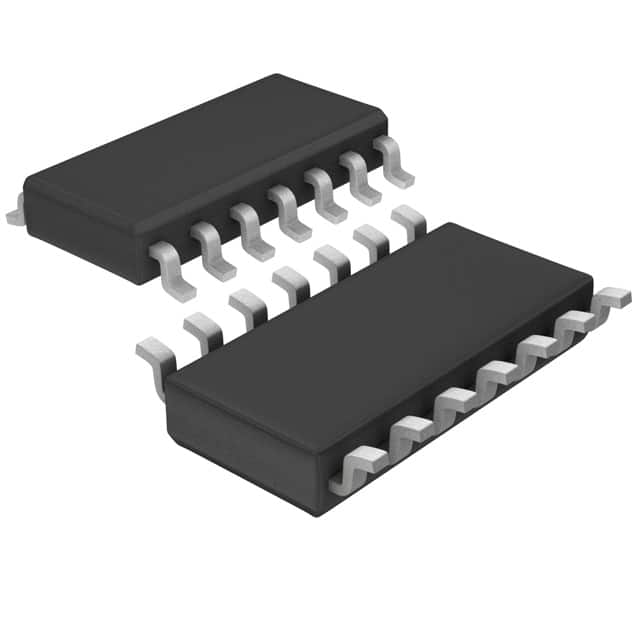
Package: The LTC2052IS#PBF is available in an industry-standard 8-pin SOIC (Small Outline Integrated Circuit) package.
Essence: The essence of the LTC2052IS#PBF lies in its ability to provide accurate and stable amplification of signals in various electronic circuits.
Packaging/Quantity: The LTC2052IS#PBF is typically sold in reels or tubes containing a quantity of 250 units per package.
Specifications
- Supply Voltage Range: 2.7V to 5.5V
- Input Offset Voltage: ±50μV (maximum)
- Input Bias Current: ±1nA (maximum)
- Gain Bandwidth Product: 1MHz
- Slew Rate: 0.6V/μs
- Quiescent Current: 60μA (typical)
- Operating Temperature Range: -40°C to 125°C
Detailed Pin Configuration
The LTC2052IS#PBF features the following pin configuration:
- OUT: Output pin
- V-: Negative power supply pin
- IN-: Inverting input pin
- IN+: Non-inverting input pin
- V+: Positive power supply pin
- NC: No connection (unused pin)
- NC: No connection (unused pin)
- GND: Ground pin
Functional Features
- Zero-drift architecture ensures minimal input offset voltage and temperature drift.
- Rail-to-rail inputs and outputs allow for maximum signal swing.
- Low noise characteristics enable high signal integrity.
- Wide supply voltage range provides flexibility in system design.
- High precision and stability make it suitable for demanding applications.
Advantages and Disadvantages
Advantages: - Exceptional accuracy and stability - Low noise performance - Wide supply voltage range - Rail-to-rail inputs and outputs - Suitable for demanding measurement and control systems
Disadvantages: - Limited gain bandwidth product compared to some specialized amplifiers - Higher quiescent current compared to ultra-low-power amplifiers
Working Principles
The LTC2052IS#PBF utilizes a zero-drift architecture, which employs techniques to minimize input offset voltage and temperature drift. This is achieved through careful circuit design and compensation techniques. The amplifier continuously adjusts its internal parameters to maintain accurate amplification of the input signal, even in the presence of environmental variations.
Detailed Application Field Plans
The LTC2052IS#PBF finds application in various fields, including: - Precision instrumentation - Sensor signal conditioning - Data acquisition systems - Medical devices - Industrial automation - Audio amplification
Detailed and Complete Alternative Models
Some alternative models that offer similar functionality to the LTC2052IS#PBF include: - AD8628 - MCP6V01 - MAX44246 - OPA333
These alternative models can be considered based on specific application requirements and design constraints.
Word count: 408 words
技術ソリューションにおける LTC2052IS#PBF の適用に関連する 10 件の一般的な質問と回答をリストします。
Sure! Here are 10 common questions and answers related to the application of LTC2052IS#PBF in technical solutions:
Q: What is LTC2052IS#PBF? A: LTC2052IS#PBF is a low-power, zero-drift operational amplifier (op-amp) manufactured by Linear Technology.
Q: What are the key features of LTC2052IS#PBF? A: The key features of LTC2052IS#PBF include low offset voltage, low input bias current, low noise, and low power consumption.
Q: What is the typical supply voltage range for LTC2052IS#PBF? A: The typical supply voltage range for LTC2052IS#PBF is between 2.7V and 5.5V.
Q: What is the input offset voltage of LTC2052IS#PBF? A: The input offset voltage of LTC2052IS#PBF is typically around 0.5µV.
Q: Can LTC2052IS#PBF be used in precision measurement applications? A: Yes, LTC2052IS#PBF is suitable for precision measurement applications due to its low offset voltage and low drift characteristics.
Q: What is the maximum output current of LTC2052IS#PBF? A: The maximum output current of LTC2052IS#PBF is typically around 20mA.
Q: Is LTC2052IS#PBF capable of driving capacitive loads? A: Yes, LTC2052IS#PBF can drive capacitive loads up to 100pF without any external compensation.
Q: Can LTC2052IS#PBF operate in single-supply configurations? A: Yes, LTC2052IS#PBF can operate in both single-supply and split-supply configurations.
Q: What is the operating temperature range for LTC2052IS#PBF? A: The operating temperature range for LTC2052IS#PBF is typically between -40°C and 85°C.
Q: Are there any application notes or reference designs available for LTC2052IS#PBF? A: Yes, Linear Technology provides application notes and reference designs on their website that can help with the implementation of LTC2052IS#PBF in various technical solutions.
Please note that the answers provided here are general and may vary depending on specific datasheet specifications and application requirements.